
Plasma processing apparatus and plasma processing method

a processing apparatus and plasma technology, applied in the direction of plasma technique, solid-state devices, electric discharge tubes, etc., can solve the problems of high substrate cost, difficult to achieve a cost reduction, and long treatment time of approximately 48 hours, and achieve high cost of substrate, high cost of consumable parts, and different crystallinity.

Active Publication Date: 2014-04-22
PANASONIC CORP
View PDF19 Cites 0 Cited by
  • Summary
  • Abstract
  • Description
  • Claims
  • Application Information

AI Technical Summary

Benefits of technology

The patent text describes a method for crystallizing a polysilicon film using a laser or a thermal plasma jet. However, both methods have limitations such as the presence of trap levels, a limitation on laser output, and a high cost. The thermal plasma jet crystallization method is a cost-effective alternative that uses an ultrahigh temperature heat source to easily crystallize a-Si films. The method is simple in structure and requires low running costs. The technical effects of this patent include the removal of limitations on substrate size and the high cost of the laser crystallization apparatus, as well as the cost-effective crystallization of polysilicon films.

Problems solved by technology

On the other hand, since the high-temperature process is the process of performing crystallization of a silicon film through solid phase epitaxy, heat treatment under a temperature of approximately 600° C. for a long time of approximately 48 hours is required.
This is an enormously long step, and involves the issue that it essentially requires great number of heat treat furnaces in order to improve the throughput of the step, which makes it difficult to achieve a reduction in costs.
In addition, since it is inevitable to use silica glass as the insulating substrate which is highly heat resistant, the cost of the substrate is high.
Therefore, it is regarded that it is not suitable for increasing the area.
However, the laser crystallization technique involves several significant issues.
Because of the presence of the trap levels, the carriers that should originally move in the active layer by application of voltage are trapped and cannot contribute to electrical conduction.
This has disadvantageous effects such as a reduction in mobility of TFTs and an increase in the threshold voltage.
Another issue is that the limitation on the laser output limits the size of the glass substrate.
However, since the current laser output is limited, in the case where the crystallization technique is adopted for a large-size substrate, e.g., of the seventh generation (1800 mm×2100 mm), it requires a long time to crystallize a piece of substrate.
Finally, since the laser crystallization apparatus has complicated device structure and the cost of the consumable parts is high, there is an issue that the apparatus cost and the running cost are high.
Thus, the TFTs using a polysilicon film crystallized by the laser crystallization apparatus become the elements whose manufacturing cost is high.
Further, since the utility required for crystallization is argon gas, electric power, and cooling water, it is the cost-effective crystallization technique in terms of the running cost also.
Though it is described that it generates thermal plasma, it generates low-temperature plasma and is not suitably structured for heat treatment.
Provided that thermal plasma is generated, since it is the capacitive coupling type using an electrode, it is considered that arc discharge would be focused on one place to make it difficult to generate thermal plasma being uniform in the longer direction.

Method used


Image

  • Plasma processing apparatus and plasma processing method
  • Plasma processing apparatus and plasma processing method
  • Plasma processing apparatus and plasma processing method

Examples


first embodiment

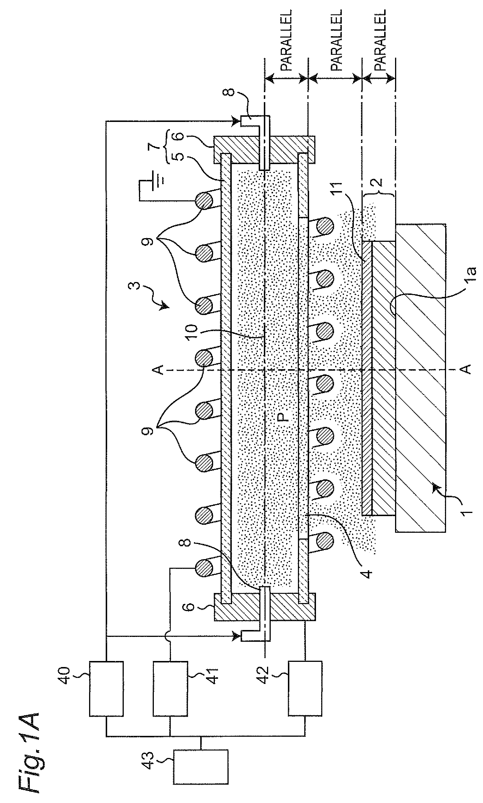
[0110]In the following, with reference to FIGS. 1A to 4, a description will be given of a first embodiment of the present invention.

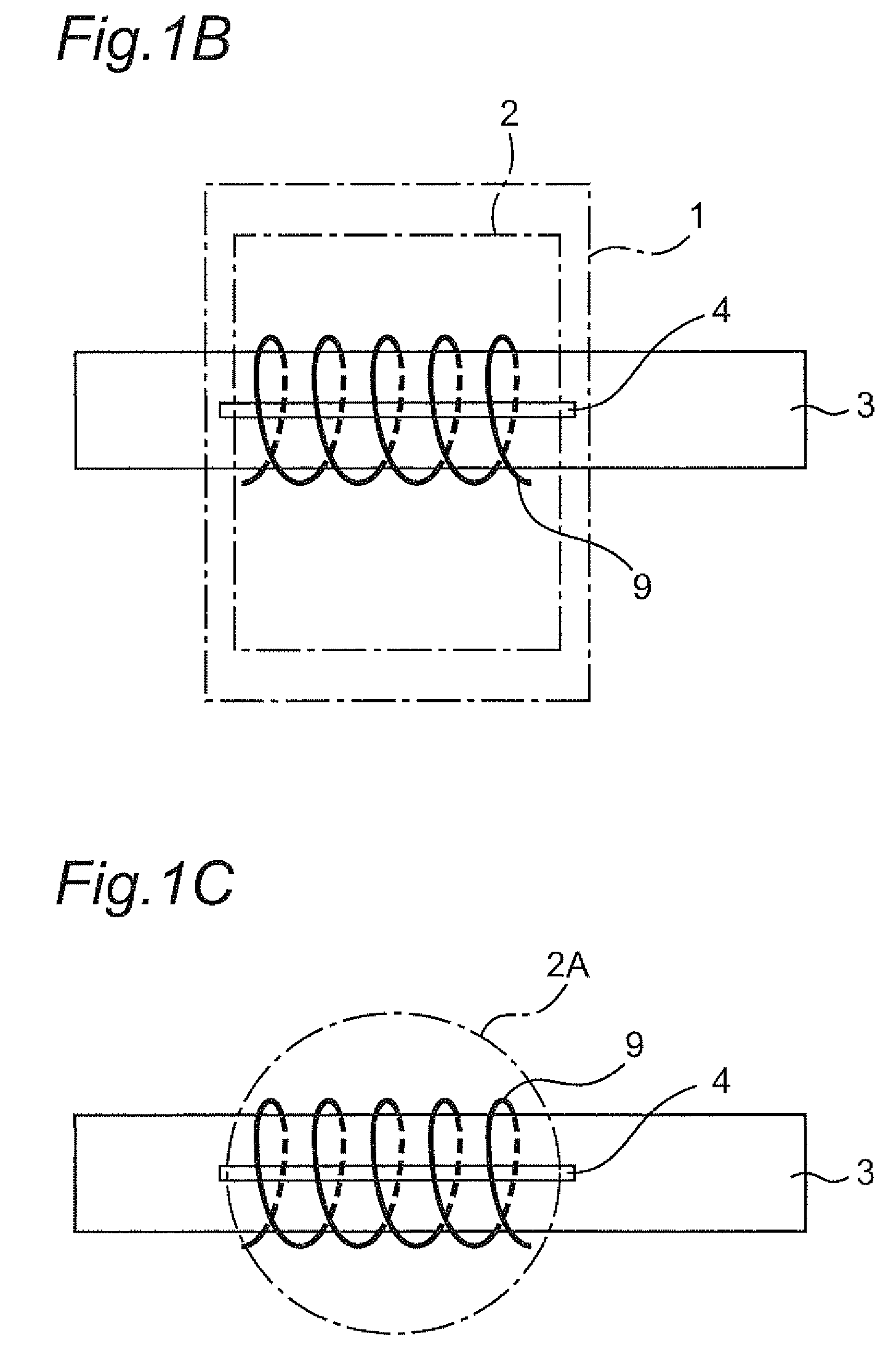
[0111]FIG. 1A shows the structure of a thermal plasma processing apparatus according to the first embodiment of the present invention. FIG. 1B is a bottom view of the plasma processing apparatus showing the relationship among the plasma processing apparatus according to the first embodiment of the present invention, a quadrilateral base material 2, and a base material placement table 1. FIGS. 1A and 1B are each a cross-sectional view taken along a plane parallel to the longer direction of an inductively coupled plasma torch unit 3, the plane including a center axis 10 of a solenoid coil 9 and being perpendicular to the surface of the base material 2. Further, FIG. 2A is a cross-sectional end view taken along dashed line A-A shown in FIG. 1A. It is to be noted that, in the following description, though the base material 2 is described as being quadrilate...

second embodiment

[0136]In the following, with reference to FIGS. 5A to 6, a description will be given of a second embodiment of the present invention.

[0137]FIG. 5A shows the structure of a thermal plasma processing apparatus according to the second embodiment of the present invention. FIG. 5A is a cross-sectional view taken along a plane parallel to the longer direction of an inductively coupled plasma torch unit 3A, the plane including a center axis 10A of a solenoid coil 9A, and being perpendicular to the surface of the base material 2. Further, FIG. 5B is a bottom view of a plasma processing apparatus showing the relationship among the plasma processing apparatus according to the second embodiment of the present invention shown in 5A, the base material, and the base material placement table. FIG. 6 is a cross-sectional end view taken along dashed line C-C shown in FIG. 5A.

[0138]In FIGS. 5A and 6, the base material 2 is placed on the base material placement face 1a of the base material placement t...

third embodiment

[0149]In the following, with reference to FIGS. 7 and 8, a description will be given of a third embodiment of the present invention.

[0150]FIG. 7 shows the structure of a thermal plasma processing apparatus according to the third embodiment of the present invention. FIG. 7 is a cross-sectional view taken along a plane parallel to the longer direction of an inductively coupled plasma torch unit 3B, the plane including a center axis 10B of a solenoid coil 9B, and being perpendicular to the surface of the base material 2. Further, FIG. 8 is a cross-sectional end view taken along dashed line D-D shown in FIG. 7.

[0151]In FIGS. 7 and 8, the base material 2 is placed on the base material placement face 1a of the base material placement table 1. The inductively coupled plasma torch unit 3B is substantially structured with a cylindrical chamber 7B and a coil case 16, which is an insulating member having a downwardly convex shape whose tip is semicircular.

[0152]The cylindrical chamber 7B is st...


PUM

PropertyMeasurementUnit
temperatureaaaaaaaaaa
temperaturesaaaaaaaaaa

Abstract

A base material is placed on a base material placement face of a base material placement table. An inductively coupled plasma torch unit is structured with a cylindrical chamber structured with a cylinder made of an insulating material and provided with a rectangular slit-like plasma jet port, and lids closing opposing ends of the cylinder, a gas jet port that supplies gas into the cylindrical chamber, and a solenoid coil that generates a high frequency electromagnetic field in the cylindrical chamber. By a high frequency power supply supplying a high frequency power to the solenoid coil, plasma is generated in the cylindrical chamber, and the plasma is emitted from the plasma jet port to the base material. While relatively shifting the plasma torch unit and the base material placement table, a base material surface can be subjected to heat treatment.

Description

TECHNICAL FIELD[0001]The present invention relates to a plasma processing apparatus and a plasma processing method, for performing plasma processing such as thermal plasma processing in which thermal plasma is emitted to a base material to process the base material, or low-temperature plasma processing in which plasma of a reactant gas is emitted or plasma and a reactant gas flow are simultaneously emitted to a base material to process the base material.BACKGROUND ART[0002]Conventionally, a semiconductor thin film such as polycrystalline silicon (poly-Si) is widely used for thin film transistors (TFTs: Thin Film Transistors) or solar cells. In particular, poly-SiTFTs are characterized by their high carrier mobility, and capability of being prepared on a transparent insulating substrate such as a glass substrate. Taking advantage of such characteristics, the poly-SiTFTs are widely used, e.g., as a switching element that structures a pixel circuit such as a liquid crystal display appa...

Claims


Application Information

Patent Timeline
Patent Type & Authority Patents(United States)
IPC IPC(8): H01L21/44H01L27/14
CPCH01L21/324H05H1/30H01J37/32825H01J37/3211H01J37/32376
Inventor OKUMURA, TOMOHIRONAKAYAMA, ICHIROSAITOH, MITSUO
Owner PANASONIC CORP
Learn More