Structure, chip for localized surface plasmon resonance sensor, localized surface plasmon resonance sensor, and fabricating methods therefor

a technology of localized surface plasmon and chip, applied in the direction of instruments, nuclear engineering, transportation and packaging, etc., can solve the problems of complex optical system of the sensor, large size, difficulty in making a sensor that is small in signal-to-noise ratio (s/n ratio) and high sensitivity, and large size of the apparatus, etc., to achieve enhanced raman scattering, high sensitivity, and high sensitivity

Inactive Publication Date: 2013-01-03
NAT INST OF ADVANCED IND SCI & TECH +1
View PDF3 Cites 18 Cited by
  • Summary
  • Abstract
  • Description
  • Claims
  • Application Information

AI Technical Summary

Benefits of technology

[0038]As stated hereinabove, according to the invention, there can be obtained an effect of providing a preferred structure and its fabrication method that is utilizable as a chip for a localized surface plasmon resonance sensor of high sensitivity, a chip for surface enhanced Raman scattering spectroscopy, a fluorescence enhancing plate, a two-photon fluorescen...

Problems solved by technology

Hence, the optical system of the sensor becomes complicated and large-sized, and there is a need of bringing a chip for sensor (glass substrate) and the prism into intimate contact with each other by means of a matching oil.
These cause noises, thu...

Method used


Image

  • Structure, chip for localized surface plasmon resonance sensor, localized surface plasmon resonance sensor, and fabricating methods therefor
  • Structure, chip for localized surface plasmon resonance sensor, localized surface plasmon resonance sensor, and fabricating methods therefor
  • Structure, chip for localized surface plasmon resonance sensor, localized surface plasmon resonance sensor, and fabricating methods therefor

Examples


example 1

Structure Fabrication-1

[0229]Such POT1 as indicated before was used as a light responsive material and a thin film of this azo polymer derivative (thickness: 100 nm) was formed on a glass substrate according to a spin coating method.

[0230]The azo polymer derivative thin film thus formed was annealed (at 150° C. for 10 minutes (normal pressure)).

[0231]1 cc of pure water was dropped over the azo polymer derivative thin film, followed by irradiation with light of a wavelength of 470 nm at an intensity of 40 mW / cm2 for five minutes.

[0232]After the irradiation, pure water was removed and the azo polymer derivative thin film after the light irradiation was air-dried, followed by observation of the surface with AFM. The results are shown in FIG. 5.

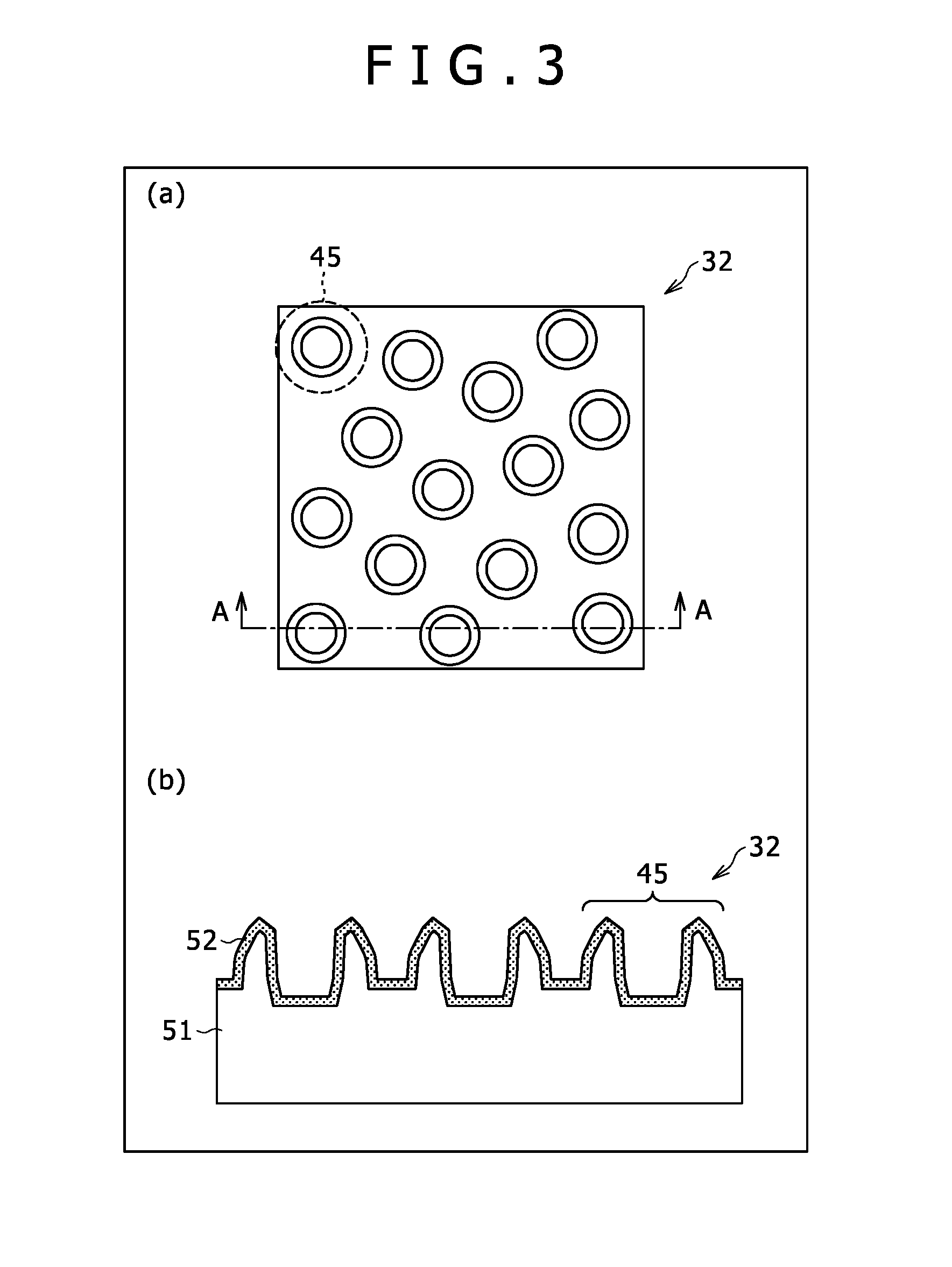
[0233]Tubular bodies of the resulting structure had an average diameter of 690 nm and a depth (average value) of 180 nm, a ratio (A / B) of inner diameter A of the openings of the tubular bodies and inner diameter B at the midpoint of the depth fro...

example 2

Structure Fabrication-2

[0236]Such an azo polymer derivative POT1 as used in Example 1 was provided as a light responsive material and coated onto a transparent substrate in a thickness of 50 nm by means of a spin coater to form an azo polymer derivative thin film.

[0237]The azo polymer derivative thin film thus formed was annealed (at 150° C. for 10 minutes (at a normal pressure)).

[0238]1 cc of pure water was dropped over the azo polymer derivative thin film and irradiated with light of a wavelength of 470 nm at an intensity of 30 mW / cm2 for five minutes.

[0239]After the irradiation, the pure water was removed and the azo polymer derivative thin film after the light irradiation was air-dried, followed by observation of the surface with AFM. The results are shown in FIG. 7.

[0240]The tubular bodies of the resulting structure had an average diameter of 350 nm and a depth (average value) of 170 nm, and a ratio (A / B) of inner diameter A of the openings of the tubular bodies and inner diame...

example 3

Structure Fabrication-3

[0242]Structures were made in the same manner as in Example 2. Of the thus formed structures, arbitrarily chosen four structures were subjected to profile measurement (Experiment Lot No. 302-1).

[0243]The procedure of Experiment Lot No. 302-1 was repeated except that after annealing (at 150° C. for 10 minutes (at a normal pressure)) prior to light irradiation, samples were allowed to stand at room temperature for 12 hours. Among the structures formed in this manner, arbitrarily chosen two structures were subjected to profile measurement (Experiment Lot No. 303-1).

[0244]These results are shown in Table 1.

TABLE 1Experiment Lot No.302-1303-1Tubular body No.123456Thickness of5050azobenzenepolymerthin film (nm)Inner450469410371371371diameter A ofopeningsof tubularbodies (nm)Inner352390273313273234diameter B atthe midpoint ofthe depth fromopenings oftubularbodies (nm)Depth (nm)185217200199194164A / B1.281.201.501.191.361.59

[0245]The invention should not be construed as...


PUM

PropertyMeasurementUnit
Thicknessaaaaaaaaaa
Thicknessaaaaaaaaaa
Lengthaaaaaaaaaa

Abstract

Implemented is a chip for localized surface plasmon resonance sensor, which is able to provide a localized surface plasmon resonance sensor of higher sensitivity. A structure of the invention is characterized by including a planar section and tubular bodies, wherein the tubular bodies are vertically arranged so that openings thereof open at the planar surface of the planar section, an average inner diameter of the openings of the tubular bodies is within a range of from 5 nm to 2,000 nm, a ratio (A/B) of inner diameter A of the openings of the tubular bodies and inner diameter B at the midpoint of the depth from the openings of the tubular bodies is within a range of from 1.00 to 1.80, and the bottom of the tubular bodies is aspherical.

Description

TECHNICAL FIELD[0001]This invention relates to a structure that is able to provide a localized surface plasmon resonance sensor of high sensitivity, a chip for localized surface plasmon resonance sensor, a localized surface plasmon resonance sensor obtained therefrom, and fabricating methods therefor. More particularly, the invention relates to a novel microstructure developed under attention to material transfer of a light responsive material based on light irradiation in the presence of a liquid, an optical processing method and a fabricating method.BACKGROUND ART[0002]60% of the human body is constituted of water and half of remaining 40% is made up of proteins. Most of cells, muscle and skin of the human body is composed of proteins. Accordingly, it has been frequently recognized that diseases are interrelated with the mutation of proteins. With cancers, influenza and other diseases, specific types of proteins increase in the body (or in the blood or the like) as the diseases pr...

Claims


Application Information

Patent Timeline
IPC IPC(8): G01N21/55B32B3/10B05D5/06
CPCG01N21/554G01N21/648Y10T428/24612Y10T428/24479G01N21/658G01N21/27B82B1/00
Inventor SEZAKI, FUMIYASUFUKUDA, TAKASHI
Owner NAT INST OF ADVANCED IND SCI & TECH
Why Eureka
Try Eureka