
Perovskite material with anion-controlled dielectric properties, thin film capacitor device, and method for manufacturing the same

a technology of anion-controlled dielectric properties and perovskite, which is applied in the direction of fixed capacitors, thin/thick film capacitors, fixed capacitor electrodes, etc., can solve the problems of difficult simultaneous to achieve large volume manufacturing reproducible quality paraelectric thin films with reasonable high tunability ratios, and achieve good voltage tunable properties and high dielectric constant

Active Publication Date: 2013-01-03
MURATA MFG CO LTD
View PDF6 Cites 20 Cited by
  • Summary
  • Abstract
  • Description
  • Claims
  • Application Information

AI Technical Summary

Benefits of technology

The present invention provides a new material, called oxynitride paraelectric nanocomposite, which has good voltage tunable properties and a high dielectric constant. The material has no measurable ferroelectricity and can be produced in large volume manufacturing processes. The resulting film has high breakdown voltage, uniform dielectric constant, low temperature coefficients of capacitance, and tunability. This material has shown promising results in applications such as high-speed electronics and optics.

Problems solved by technology

However, there have been no reports of deposition and characterization of oxynitride polycrystalline ABO2N1 or ABO3-γNγ thin films grown on Pt electrodes on common large size commercially available substrates nor any C-V or I-V characteristics of any ferroelectric oxynitride perovskite, except for the dielectric constants of LaTiO2N1 and BaTaO2N1 thin films at zero dc bias.
All of the commonly known deposition methods of BST films, and particular solutions for achieving high voltage tunability and / or high capacitance density required for achieving better performance variable capacitors and / or high density decoupling thin film capacitors, typically require using very high deposition temperatures of about 800° C. or higher, very high post-deposition annealing temperatures between 800° C. and 900° C., and thicker BST dielectric layers, typically between 200 nm and 600 nm, all of which make it very difficult to simultaneously achieve large volume manufacturing reproducible quality paraelectric thin films with reasonably high tunability ratios, i.e., tunability ratios of at least 4-6:1, under applied DC biases below 6-8 Volts, low dielectric loss, i.e., of less than 1% at 1 KHz or 1 GHz, which is typically only possible at lower deposition temperatures of about 600° C. to about 650° C. The deposition of oxynitride perovskite thin films requires using epitaxially matching substrates which are not available in large manufacturing sizes and typically obtained oxynitride perovskite materials are not stable above 600° C. if annealed in oxygen atmospheres.

Method used


Image

  • Perovskite material with anion-controlled dielectric properties, thin film capacitor device, and method for manufacturing the same
  • Perovskite material with anion-controlled dielectric properties, thin film capacitor device, and method for manufacturing the same
  • Perovskite material with anion-controlled dielectric properties, thin film capacitor device, and method for manufacturing the same

Examples


Embodiment Construction

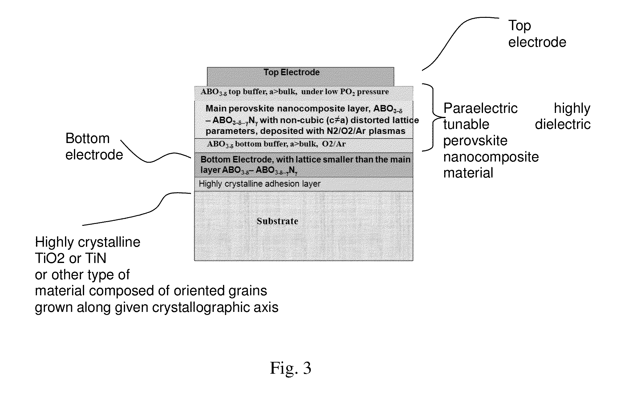
[0058]A highly tunable ferroelectric variable capacitor (varactor) structure according to a preferred embodiment of the present invention, as shown in FIG. 3, preferably includes a single layer or multiple layers of crystalline composite paraelectric material including nano-regions containing rich N3− anions dispersed in a nano-grain sized matrix of crystalline oxide perovskite material, wherein (ABO3-δ)α-(ABO3-δ-γNγ)1-α (0.011-x,Srx)TiO3-δ)α—(Ba1-x,Srx)TiO3-δ-γNγ)1-α or BSTON-BSTO (0.5<1-x<0.8), or a multilayer combination of such oxide or oxynitride nanocomposite perovskites, deposited between bottom and top electrode layers.

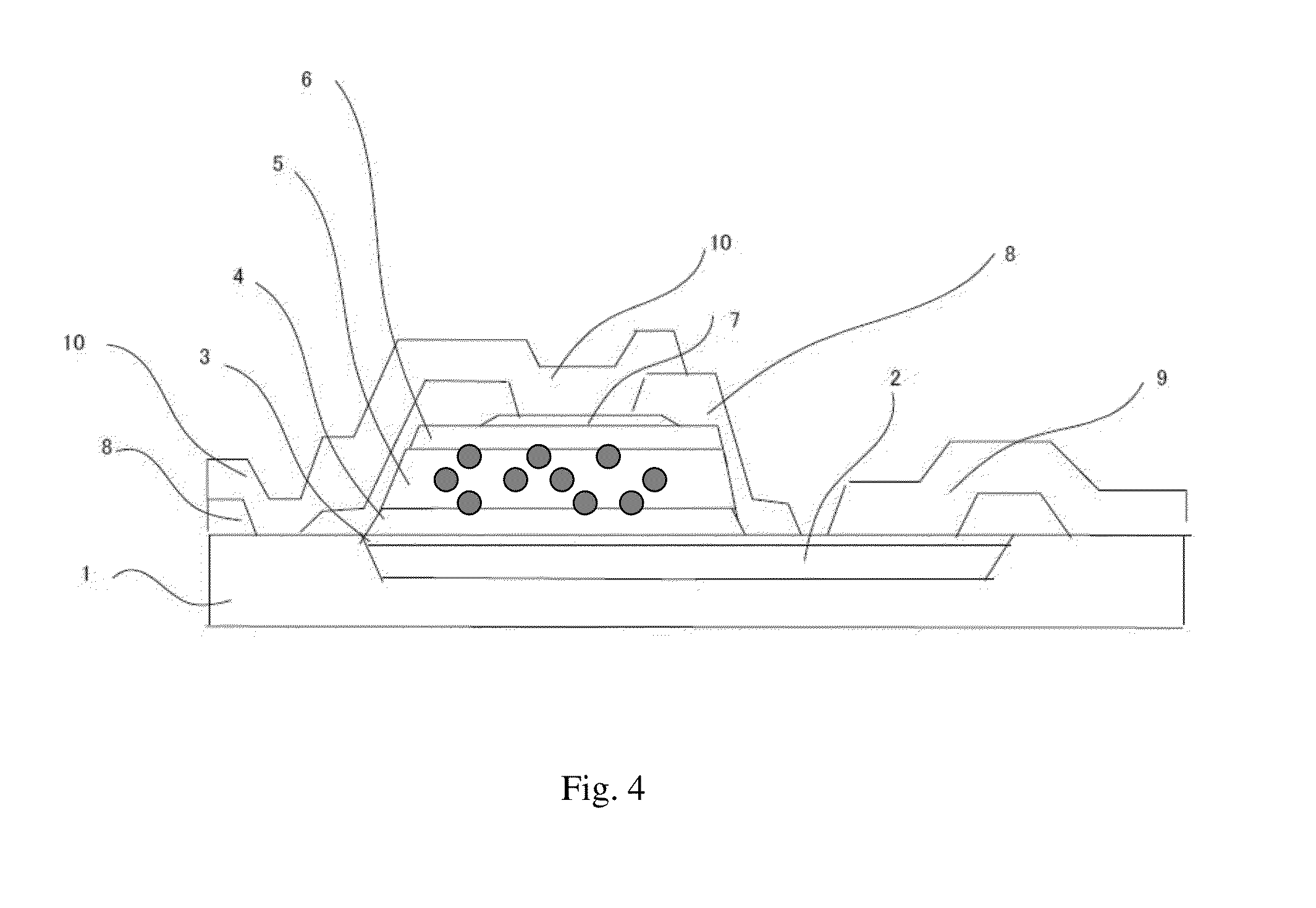
[0059]FIG. 3 and FIG. 4 are schematic cross-sections of the highly tunable ferroelectric variable capacitor including a substrate 1 preferably made of sapphire, LiNbO3, LiTaO3, Al2O3 ceramic, LTCC, Si, (silicon on insulator) SOI, GaAs, SiC, GaN, or other suitable materials, for example. On the substrate 1, a highly crystalline and very thin adhesion layer pref...


PUM

PropertyMeasurementUnit
thicknessaaaaaaaaaa
electric fieldaaaaaaaaaa

Abstract

A crystalline perovskite crystalline composite paraelectric material includes nano-regions containing rich N3− anions dispersed in a nano-grain sized matrix of crystalline oxide perovskite material, wherein (ABO3-δ)α-(ABO3-δ-γNγ)1-α. A represents a divalent element, B represents a tetravalent element, γ satisfies 0.005≦γ≦1.0, 1-α satisfies 0.05≦1-α≦0.9, and 1-α is an area ratio between the regions containing rich N3− anions and the matrix of remaining oxide perovskite material.

Description

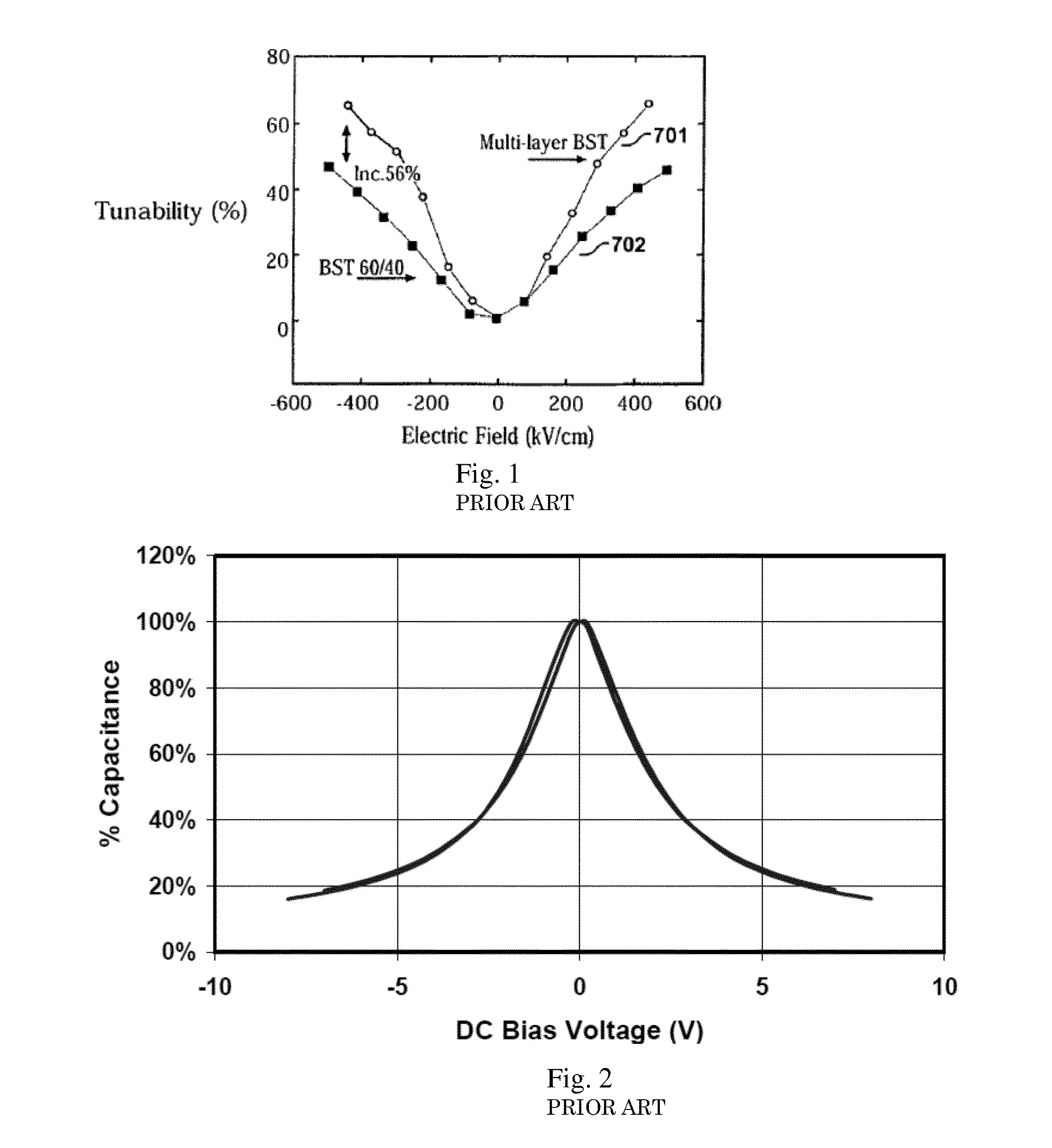
BACKGROUND OF THE INVENTION[0001]1. Field of the Invention[0002]The present invention relates to thin film materials, suitable for ferroelectric tunable devices and / or decoupling thin film capacitors based on such materials, and methods of manufacturing thin film devices, and more particularly, to paraelectric perovskite oxynitride nanocomposite materials and methods of making such materials for use in forming varactor devices with improved voltage tunabilities and high capacitance density thin film decoupling capacitors.[0003]2. Description of the Related Art[0004]In order to achieve maximum tunability of a ferroelectric varactor, a maximum voltage must be applied to induce a change in the dielectric constant needed to produce the maximum possible shift in capacitance. FIG. 1 illustrates an example of a typical tunability achieved with a ferroelectric varactor using a thin-film ferroelectric material, such as (Ba,Sr)TiO3. FIG. 1 corresponds to FIG. 7 of U.S. 2009 / 0069274.[0005]U.S....

Claims


Application Information

Patent Timeline
Patent Type & Authority Applications(United States)
IPC IPC(8): C04B35/468C04B35/00C04B35/46C04B35/465C04B35/462C04B35/47C04B35/057C23C14/34H01G7/06C04B35/48B82Y30/00
CPCC01G23/006C01P2002/34C01P2002/52C01P2002/54H01L28/56H01L21/02197H01L21/02266H01G7/06H01B3/10C01P2006/40C23C14/34H01G4/008H01G4/085H01G4/10H01G4/33
Inventor KOUTSAROFF, IVOYLHIGAI, SHINICHIANDO, AKIRA
Owner MURATA MFG CO LTD
Learn More