Unlock instant, AI-driven research and patent intelligence for your innovation.

Epoxy resin composition for semiconductor encapsulation and semiconductor device using the same

Active Publication Date: 2013-01-31
NITTO DENKO CORP
View PDF6 Cites 13 Cited by
  • Summary
  • Abstract
  • Description
  • Claims
  • Application Information

AI Technical Summary

Benefits of technology

The object of this patent text is to provide an epoxy resin composition for semiconductor encapsulation that can reduce the warping of the substrate while inhibiting an increase in the high-temperature modulus of the resin.

Problems solved by technology

The linear expansion coefficient of the encapsulating resin itself may be reduced (that is, be made close to the linear expansion coefficient of the substrate to reduce the difference between both members) by increasing the content of the inorganic filler, but the high-temperature modulus of the encapsulating resin rises (the difference from the substrate increases) and therefore, the effect in terms of inhibiting warpage generation is insufficient.
Also, blending of other various additives is being studied, but as for the inhibition of warpage generation, a satisfactory effect is not obtained at present.

Method used


Image

  • Epoxy resin composition for semiconductor encapsulation and semiconductor device using the same
  • Epoxy resin composition for semiconductor encapsulation and semiconductor device using the same
  • Epoxy resin composition for semiconductor encapsulation and semiconductor device using the same

Examples


examples

[0057]In the following, Examples are described together with Comparative Examples. However, the present invention is not limited to these Examples. In Examples and Comparative Examples, “wt %” means % by weight.

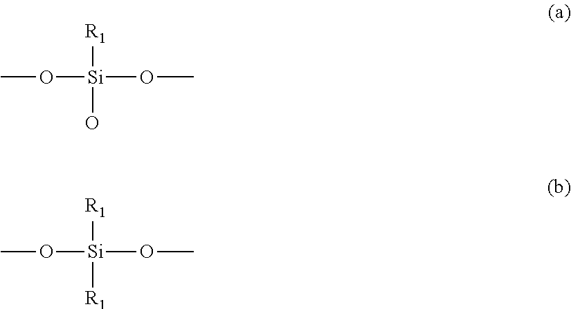
[0058]The components shown below were prepared. Incidentally, Silicone Compounds d1 to d18 are a compound having structural units represented by formulae (a) and (b), and the organic group (R1) contained is shown by each compound. Each of the silicone compounds was produced by synthesis in accordance with the above-described synthesis method, and, for example, the kind of the organic substituent and the condensation reaction time were appropriately adjusted to give the desired specific gravity and alkoxy group content.

[Epoxy Resin a1]

[0059]Biphenyl-type epoxy resin (epoxy equivalent: 192, melting point: 105° C.)

[Epoxy Resin a2]

[0060]Triphenylmethane-type polyfunctional epoxy resin (epoxy equivalent: 169, melting point: 60° C.)

[Phenol Resin b1]

[0061]Biphenyl aralkyl-type pheno...

example)

[Silicone Compound d10] (Example)

[0074]Specific gravity: 1.11, alkoxy group content: 15 wt % (methoxy group), organic substituent: phenyl group / methyl group

[Silicone Compound d11] (Comparative Example)

[0075]Specific gravity: 1.07, alkoxy group content: 25 wt % (methoxy group), organic substituent: methyl group

[Silicone Compound d12] (Comparative Example)

[0076]Specific gravity: 1.07, alkoxy group content: 17 wt % (methoxy group), organic substituent: phenyl group / methyl group

[Silicone Compound d13] (Comparative Example)

[0077]Specific gravity: 1.25, alkoxy group content: 0 wt %, organic substituent: phenyl group

[Silicone Compound d14] (Comparative Example)

[0078]Specific gravity: 1.25, alkoxy group content: 0 wt %, organic substituent: phenyl group / propyl group

[Silicone Compound d15] (Comparative Example)

[0079]Specific gravity: 1.33, alkoxy group content: 0 wt %, organic substituent: phenyl group / methyl group

[Silicone Compound d16] (Comparative Example)

[0080]Specific gravity: 1.25, alk...

case of example 13

(3) In Case of Example 13 and Comparative Examples 13′ and 14

[0095]

Reduction ratio of linear expansion coefficient per amount of silicone compound blended (CTE2 reduction ratio; ppm / wt %)=[(CTE2 of each sample−CTE2 of resin system 3) / amount of silicone compound blended]×100

[0096]The sample was rated “A” when the value above was smaller than the value (CTE2 reduction ratio caused by the addition of the inorganic filler) obtained by subtracting the CTE2 value of a sample composed of a standard resin system (resin systems 1, 2 and 3 in which the silicone compound was not added) from the CTE2 value of a test piece (Comparative Example 1, Comparative Example 11, Comparative Example 13) produced by additionally adding the same amount of the inorganic filler in place of the silicone compound (subtraction) and dividing the obtained value by the amount of the additionally added inorganic filler (division) (the value of CTE2 reduction ratio was from −4.5 to −3.05), rated “AA” when greatly sma...


PUM


Abstract

The present invention relates to an epoxy resin composition for semiconductor encapsulation, including the following components (A) to (D): (A) an epoxy resin; (B) a phenol resin; (C) an inorganic filler, and (D) a silicone compound containing an alkoxy group directly bonded to silicon atom in an amount of 10 to 45 wt % based on the entire silicone compound and having a specific gravity of 1.10 to 1.30.

Description

FIELD OF THE INVENTION[0001]The present invention relates to a semiconductor device reduced in warpage generation and excellent in the mounting reliability and soldering resistance. More specifically, the present invention relates to an epoxy resin composition for semiconductor encapsulation, which is used as an encapsulating material of a single-sided encapsulation-type semiconductor device, and a semiconductor device using the same.BACKGROUND OF THE INVENTION[0002]Conventionally, a semiconductor device has been fabricated by encapsulating various semiconductor elements such as transistor, IC and LSI with a ceramic package or the like, but in view of cost and mass productivity, resin encapsulation using a plastic package is recently predominating. In this type of resin encapsulation, an epoxy resin composition has been heretofore used and achieved good results.[0003]However, technical innovation in the semiconductor field brings an increase in the integration degree and at the same...

Claims


Application Information

Patent Timeline
IPC IPC(8): C08L63/00H01L23/29
CPCC08L61/06C08G77/18C08L63/00H01L2924/10253C08G59/621H01L2924/3511H01L2924/15311H01L2224/73265H01L2224/48227H01L2224/32225H01L23/3128H01L23/295C08K3/0033C08L83/04H01L2924/00012H01L2924/00H01L24/73C08K3/013C08G59/18C08K5/5415H01L23/29
Inventor IWASHIGE, TOMOHITOICHIKAWA, TOMOAKIFUSUMADA, MITSUAKISUGIMOTO, NAOYA
Owner NITTO DENKO CORP
Features
  • R&D
  • Intellectual Property
  • Life Sciences
  • Materials
  • Tech Scout
  • Unparalleled Data Quality
  • Higher Quality Content
  • 60% Fewer Hallucinations
Learn More