Low Volumetric Density Betavoltaic Power Device

Active Publication Date: 2013-02-07
WIDETRONIX
View PDF9 Cites 11 Cited by
  • Summary
  • Abstract
  • Description
  • Claims
  • Application Information

AI Technical Summary

Benefits of technology

[0009]One embodiment of this invention is a betavoltaic cell that has been fabricated using a semiconductor that includes, but is not limited to, Silicon Carbide (SiC), Silicon (Si), Gallium Arsenide (GaAs), Indium Gallium Arsenide (InGaAs), Gallium Nitide (GaN), Gallium Phosphide (GaP), or Diamond, and uses through wafer via holes or other fabrication techniques to form both positive (+ve) and negative (−ve) contact

Problems solved by technology

Chemical batteries, while they can be scaled down to the sizes required for these applications, end up, for lack of fuel volume at this size, having very short lifetimes. The challenge for the design and production of a betavoltaic for these applications is to take the high energy density inherent in the radioiso

Method used


Image

  • Low Volumetric Density Betavoltaic Power Device
  • Low Volumetric Density Betavoltaic Power Device
  • Low Volumetric Density Betavoltaic Power Device

Examples


Embodiment Construction

[0013]In one embodiment of the invention, a metal tritide is fabricated on the surface of a semiconductor diode convertor, to form a single unit betavoltaic cell. In another embodiment of the invention, the metal can be, but is not limited to, titanium, scandium, yttrium, hafnium, erbium, and zirconium, and the semiconductor used to fabricate the diode convertor can be, but is not limited to, SiC, GaN, GaAs, GaP, InGaAs, and diamond.

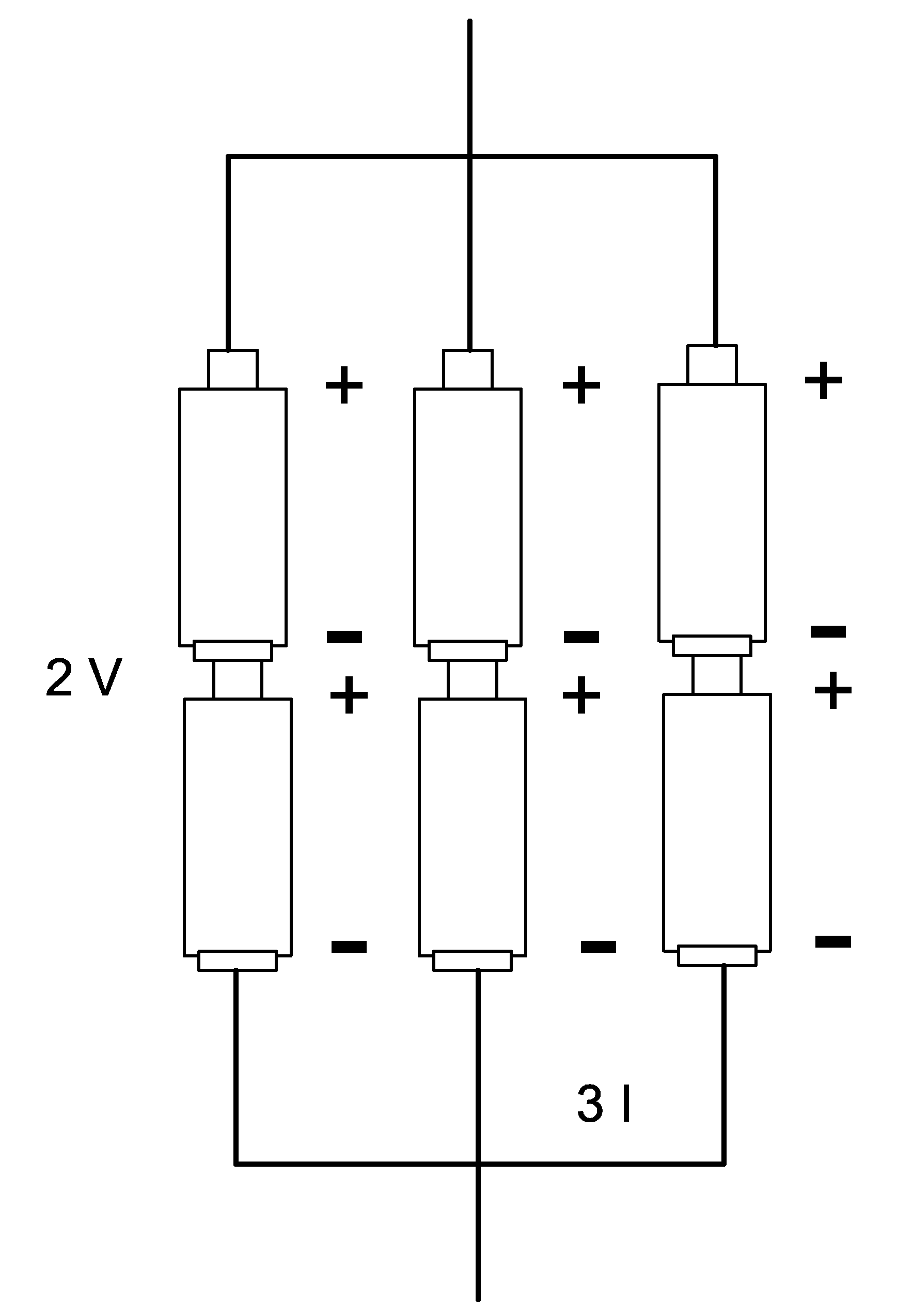
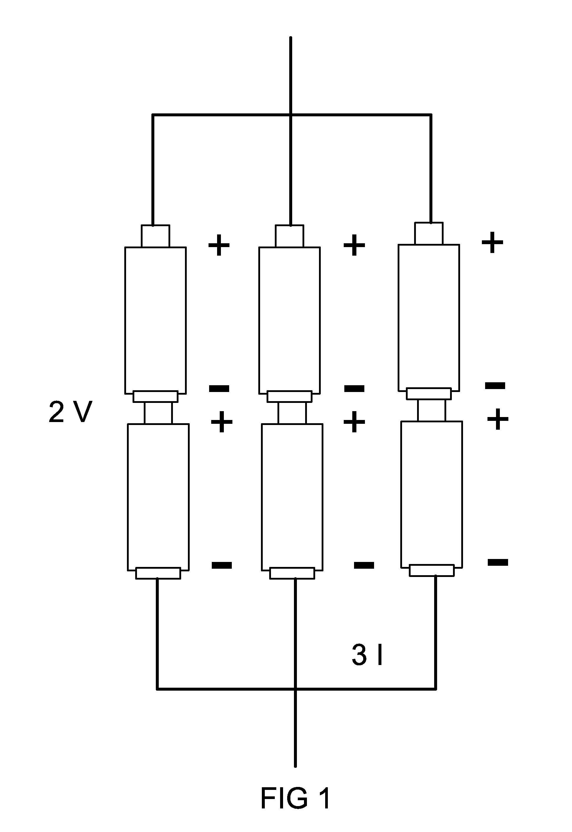
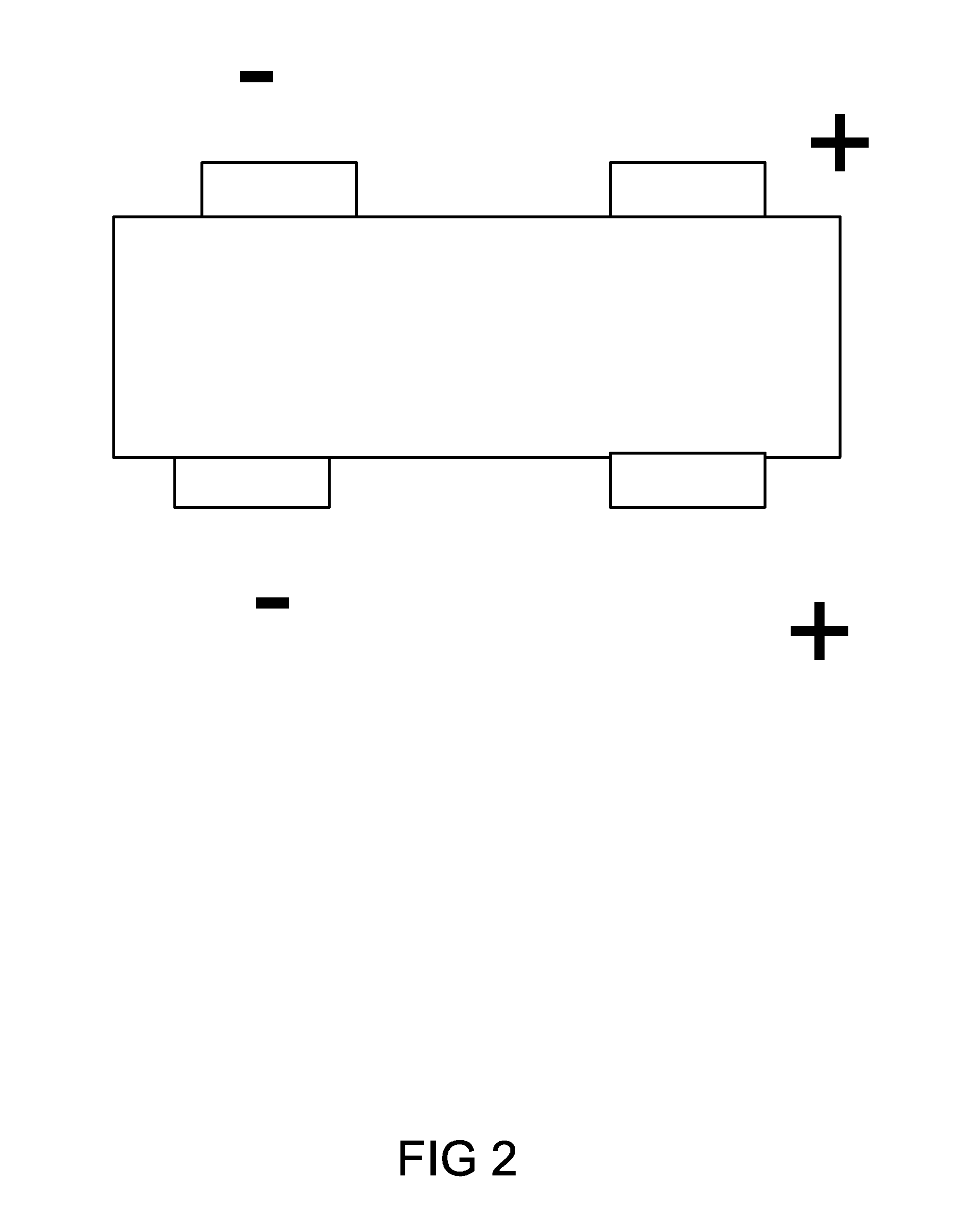
[0014]In a further embodiment of the invention, wafer through via hole technology or some other through or around wafer metal, or other conducting material, front to back connecting technology is used to create both positive (+ve) and / or negative (−ve) contacts on the front and / or back of the device cell (See the Appendices 1-3). This new cell with front and / or backside positive and negative contacts can have at least three different configurations. In one embodiment, the top cell of the stack will have only a positive contact on the top and both negativ...


PUM


Abstract

One example is a betavoltaic cell that has been fabricated using a semiconductor that includes, but is not limited to, Silicon Carbide (SiC), Silicon (Si), Gallium Arsenide (GaAs), Indium Gallium Arsenide (InGaAs), Gallium Nitide (GaN), Gallium Phosphide (GaP), or Diamond, and uses through wafer via holes or other fabrication techniques to form both positive (+ve) and negative (−ve) contacts on the front and back sides of the cell. In another example, several of these cells with +ve and −ve contacts on the front and back sides of the cell are arranged vertically and/or horizontally to form customized parallel and/or series combinations that produce a close packed, energy dense betavoltaic composite unit, with increased power outputs relative to a single cell. In another example, tritium or a metal tritide is used as the radioisotope source for the cells.

Description

RELATED APPLICATIONS[0001]This application is based on a prior provisional application, Ser. No. 61 / 515,938, with the same title, inventor, and assignee, filed on 7 Aug. 2011, claiming benefit as its priority date, whose teaching is incorporated herein, by reference.[0002]This application is also related to “HIGH POWER DENSITY BETAVOLTAIC BATTERIES”, which we filed on 6 Aug. 2010, as Ser. No. 12 / 851,555, and the disclosure of which is incorporated herein, by reference. Ser. No. 12 / 851,555, in turn, is based on a U.S. provisional application Ser. No. 61 / 231,863, filed on 6 Aug. 2009, as its priority date.INTRODUCTION[0003]Betavoltaics are radioisotope batteries that harvest the energy from beta radiation sources and perform direct conversion of this energy to electrical power. The electrical power output of a betavoltaic battery is in the form of a value of current at a particular value of voltage. The range of the overall power output is typically from nano Watts (nW) to milli Watts...

Claims


Application Information

Patent Timeline
IPC IPC(8): G21H1/06
CPCA61N1/378G21H1/06
Inventor THOMAS, CHRIS
Owner WIDETRONIX
Why Eureka
Try Eureka