Manufacturing method of piezoelectric film element, piezoelectric film element and piezoelectric device

Active Publication Date: 2013-02-14
SUMITOMO CHEM CO LTD
View PDF3 Cites 16 Cited by
  • Summary
  • Abstract
  • Description
  • Claims
  • Application Information

AI Technical Summary

Benefits of technology

[0034]According to one embodiment of the invention, a manufacturing method of a piezoelectric film element can be provided that is capable of enhancing an etching rate even when the microfabricat

Problems solved by technology

Where the microfabrication is carried out by using the above-mentioned dry etching process, it may take a long time of 1 hour or more for processing a typical KN

Method used


Image

  • Manufacturing method of piezoelectric film element, piezoelectric film element and piezoelectric device
  • Manufacturing method of piezoelectric film element, piezoelectric film element and piezoelectric device
  • Manufacturing method of piezoelectric film element, piezoelectric film element and piezoelectric device

Examples


first embodiment

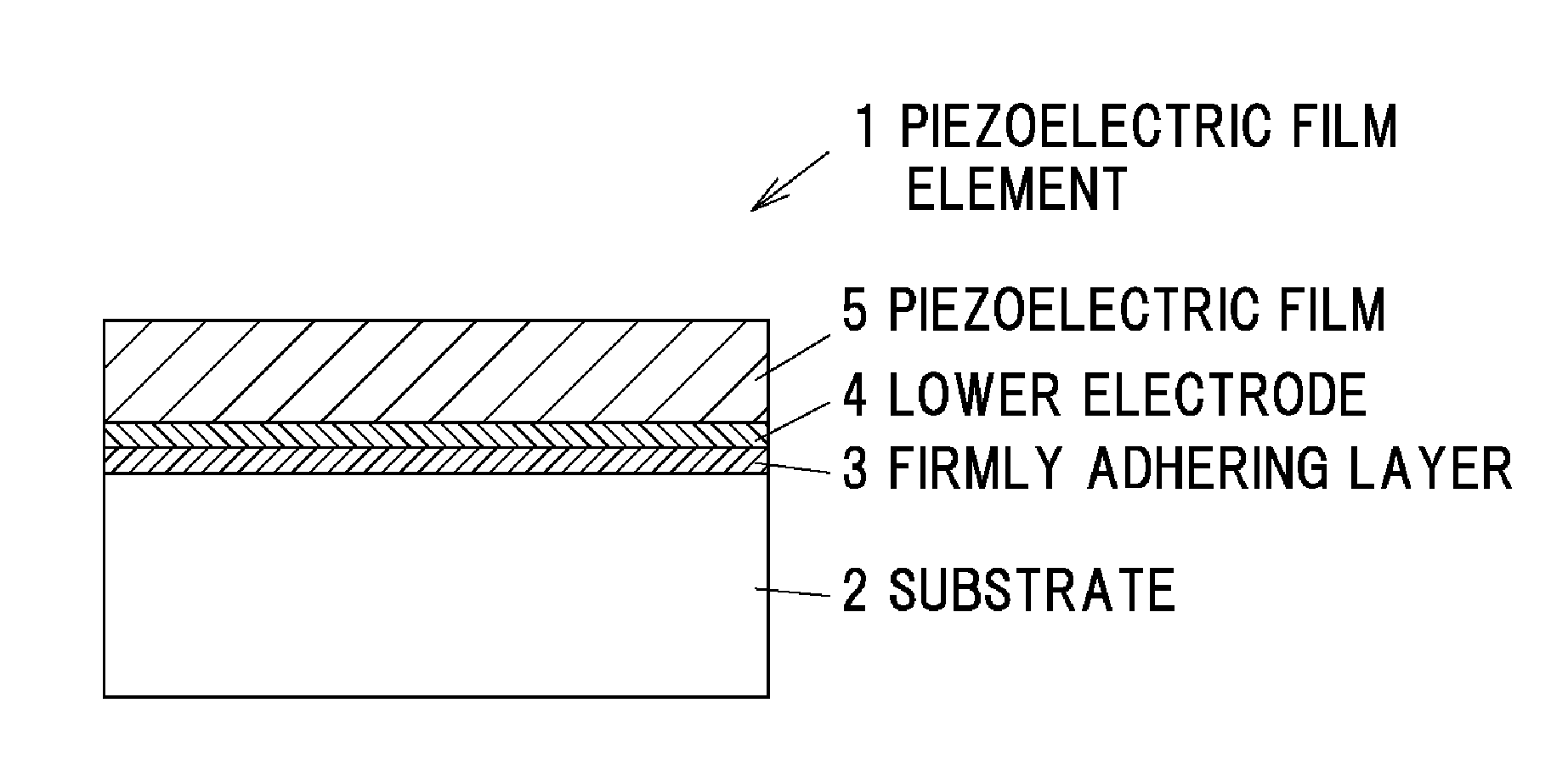
[0045]FIG. 1 is a cross-sectional view schematically showing a piezoelectric film element according to a first embodiment of the invention.

[0046]The piezoelectric film element 1 includes a substrate 2, a firmly adhering layer 3 formed on the substrate 2, a lower electrode 4 formed on the firmly adhering layer 3, and a piezoelectric film 5 formed on the lower electrode 4 in a predetermined pattern by dry etching.

[0047]As the substrate 2, for example, a Si substrate, a MgO substrate, a SrTiO3 substrate, a SrRuO3 substrate, a glass substrate, a quartz glass substrate, a GaAs substrate, a GaN substrate, a sapphire substrate, a Ge substrate, a metal substrate such as a stainless substrate, can be used. In the embodiment, the Si substrate that is low cost and is industrially proven is used. In addition, a (001) plane Si substrate with a thermally-oxidized film can be used. Also, Si substrate with a different plain direction, a Si substrate without the thermally-oxidized film and a SOI sub...

second embodiment

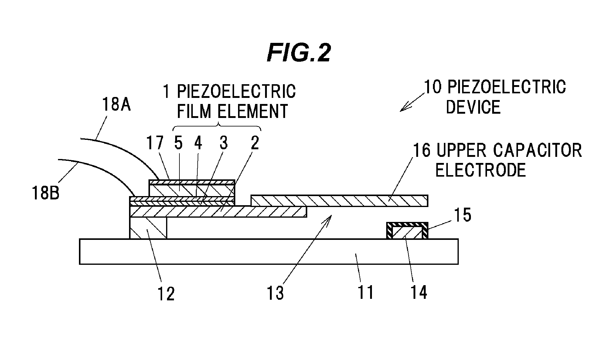
[0065]FIG. 2 is a cross-sectional view schematically showing a piezoelectric device according to a second embodiment of the invention. The second embodiment relates to the case that the piezoelectric film element 1 according to the first embodiment is applied to a variable capacitor.

[0066]The piezoelectric device 10 includes a device substrate 11, an insulation layer 12 formed on the device substrate 11, and a piezoelectric film element 1 similar to that of the first embodiment formed on the insulation layer 12. The device substrate 11 and the insulation layer 12 function as a supporting member that supports one end portion of the piezoelectric film element 1.

[0067]The piezoelectric film element 1 is configured similarly to that of the first embodiment, such that the firmly adhering layer 3, the lower electrode 4 and the piezoelectric film 5 are formed on the substrate 2. In a case of the second embodiment, an upper electrode 17 is formed on the piezoelectric film 5 of the piezoelec...

example 1

[0073]First, a manufacturing method of a piezoelectric film element according to Example 1 will be explained.

[0074](1) Preparation of Substrate

[0075]As the substrate 2, a wafer of a Si substrate with a thermally-oxidized film (oriented in the direction of (100) plane, 0.525 mm in thickness, the thermally-oxidized film of 205 nm in thickness, 4 inches in wafer size) was used.

[0076](2) Formation of Lower Electrode

[0077]First, the firmly adhering layer 3 comprised of Ti having a thickness of 2.3 nm was formed as a film on the substrate 2 by a RF magnetron sputtering method. Next, the lower electrode 4 comprised of Pt having a thickness of 215 nm was formed on the firmly adhering layer 3 by a RF magnetron sputtering method. The Ti firmly adhering layer 3 and the lower electrode 4 were formed as a film under the conditions of substrate temperature of 100 to 350 degrees C., RF power of 200 W, introduced gas of Ar atmosphere, pressure of 2.5 Pa, and film-forming time of 1 to 3 minutes for ...


PUM


Abstract

A manufacturing method of a piezoelectric film element includes forming a piezoelectric film including a lead-free alkali niobate based compound having a perovskite structure represented by a compositional formula of (K1-xNax)NbO3 on a substrate, and dry-etching the piezoelectric film by using a low-pressure plasma including a fluorine system reactive gas.

Description

[0001]The present application is based on Japanese patent application No. 2011-174981 filed on Aug. 10, 2011, the entire contents of which are incorporated herein by reference.BACKGROUND OF THE INVENTION[0002]1. Field of the Invention[0003]This invention relates to a manufacturing method of piezoelectric film element, a piezoelectric film element and a piezoelectric device.[0004]2. Description of the Related Art[0005]A piezoelectric material is processed so as to form various piezoelectric elements in accordance with a variety of the intended uses, in particular, is widely used as a functional electronic component such as an actuator that allows an object to be changed in shape when an electric voltage is applied thereto, a sensor that generates an electric voltage due to the change in shape of the element.[0006]As the piezoelectric material that is used for the application of the actuator and the sensor, a lead-based ceramics that has a large piezoelectric property, in particular, ...

Claims


Application Information

Patent Timeline
IPC IPC(8): H01L41/04H01L41/22H01L41/047
CPCH01G5/18H01L41/332H01L41/1873H01L41/094H10N30/877H10N30/1051H10N30/2042H10N30/8542H10N30/082H10N30/87
Inventor HORIKIRI, FUMIMASASHIBATA, KENJISUENAGA, KAZUFUMIWATANABE, KAZUTOSHINOMOTO, AKIRA
Owner SUMITOMO CHEM CO LTD
Why Eureka
Try Eureka