Light emitting device having group iii-nitride current spreading layer doped with transition metal or comprising transition metal nitride

a technology of nitride and current spreading layer, which is applied in the direction of metal/alloy conductors, basic electric elements, and conductors. it can solve the problems of nitride film cracks, tensile strain builds up with si doping level, and low dopant concentration, so as to reduce local lattice strain and high dopant concentration

Inactive Publication Date: 2013-02-28
ZHEJIANG INVENLUX TECH
View PDF22 Cites 33 Cited by
  • Summary
  • Abstract
  • Description
  • Claims
  • Application Information

AI Technical Summary

Benefits of technology

[0005]To solve the problems discussed above, the present invention provides a light-emitting device, such as a light-emitting diode (LED), having a group III-nitride current spreading layer which is doped with transition metal. Throughout this specification the terms “III nitride” and “IIIA nitride” are exchangeably used. The inventor of the present invention discovers that using transition metal as dopants for group III nitrides has numerous advantages compared with traditional dopants such as silicon as will be discussed in more details later. According to the present invention transition metals are used as dopants for AlInGaN group IIIA nitrides such as GaN. These dopants include transition metals from groups IIIB-VIB of the periodic table of the elements, such as Scandium (Sc), Yttrium (Y), Titanium (Ti), Zirconium (Zr), Hafnium (Hf), Vanadium (V), Niobium (Nb), Tantalum (Ta), Chromium (Cr), Molybdenum (Mo), and Tungsten (W).
[0006]According to the present invention, the dopant concentration or equivalent dopant concentration of these transition metals in an AlInGaN nitride layer can be in the range of 1017-1022 cm−3. High dopant concentration is enabled in the present invention by reducing local lattice strain between the dopant and the host lattice.

Problems solved by technology

It is noted that such a high Si-doping level, much higher than the Mott transition doping level (˜2×1018 cm−3 for GaN), is detrimental, in one hand to the material quality hence the LED's IQE, on the other hand to the light extraction efficiency because of increased light absorption due to heavy doping.
However, because of the local strain arising from the large difference between Si—N and Ga—N bonds, Si doping effectiveness tends to decrease when Si dopant concentration increases, with more and more Si atoms taking interstitial lattice positions.
A commonly observed detrimental effect of Si-doping in GaN is that tensile strain builds up with Si doping level.
Heavily doping with Si eventually results in nitride film cracks and crystal quality deterioration.
This high resistivity limits current spreading and sets up a bottleneck for GaN based high-power LEDs.

Method used


Image

  • Light emitting device having group iii-nitride current spreading layer doped with transition metal or comprising transition metal nitride
  • Light emitting device having group iii-nitride current spreading layer doped with transition metal or comprising transition metal nitride
  • Light emitting device having group iii-nitride current spreading layer doped with transition metal or comprising transition metal nitride

Examples


Embodiment Construction

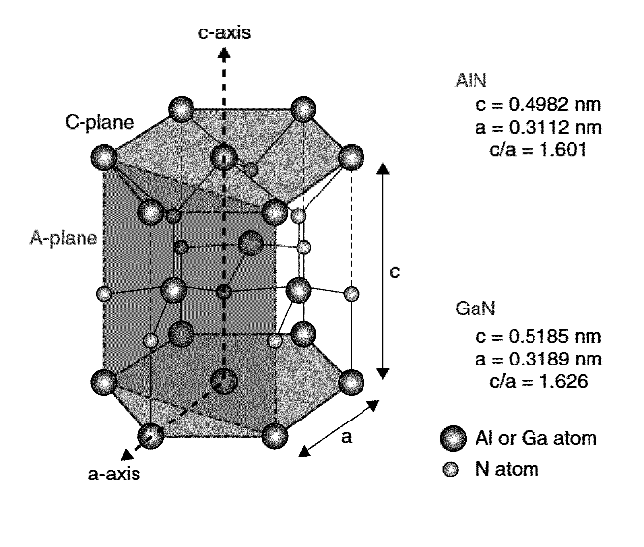
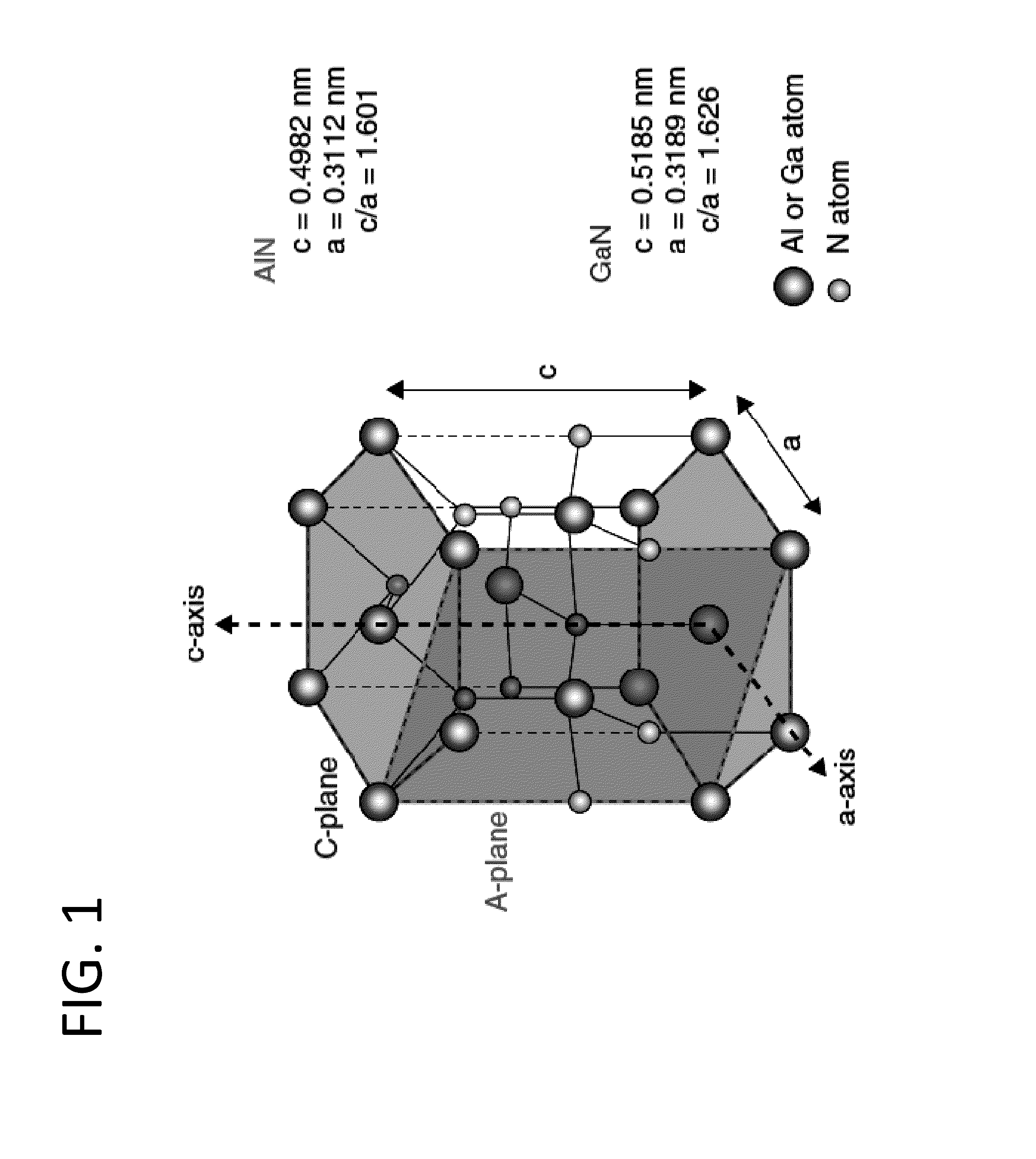
[0069]FIG. 1 illustrates a unit cell for group IIIA-nitride with wurtzite crystal structure. As seen, the (0001) surface is metal atom-terminated. For wurtzite GaN, the (0001) surface is Ga-terminated. The in-plane lattice constant a for AlInGaN is from 3.111-3.544 Å, depending on Al—, In—, Ga— compositions.

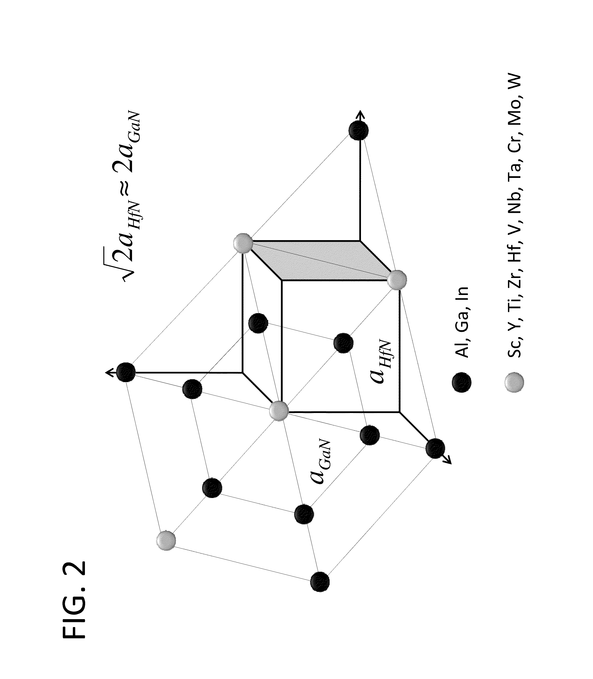
[0070]Metallic nitrides including groups IIIB-VIB nitrides tend to take cubic lattice crystal structure (NaCl structure) with lattice constant around 4.5-4.6 Å. This means that cubic group IIIB-VIB nitrides and wurtzite group IIIA nitrides can mix together with small in-plane lattice mismatch when proper coincident-site lattice is arranged for (0001) wurtzite structure and (111) cubic structure. Referring to FIG. 2, taking cubic HfN and wurtzite GaN for example, when (111) HfN formed on (0001) GaN, coincident-site lattice involving two GaN unit cells and one HfN unit cell results in a very small in-plane lattice mismatch:

2aGaN-2aHfN2aGaN=-0.21%.

[0071]This means that high-quality ...


PUM

PropertyMeasurementUnit
thicknessaaaaaaaaaa
thicknessaaaaaaaaaa
reflectivityaaaaaaaaaa

Abstract

A light-emitting device, such as a light-emitting diode (LED), has a group III-nitride current spreading layer which is either doped with transition metal, or comprises alternating transition metal nitride layer and group III-nitride layer. Also provided is a light-emitting device, such as a light-emitting diode (LED), having a quantum well doped with transition metal. Also provided is a method of forming transition-metal containing AlInGaN electrical conductive material.

Description

1. FIELD OF THE INVENTION[0001]The present invention relates in general to light-emitting device having group III-nitride layer, more particularly to light-emitting device having group III-nitride layer doped with transition metal or comprising transition metal nitride and method for fabricating the same.2. DESCRIPTION OF THE RELATED ART[0002]III-nitride based light-emitting devices such as light-emitting diodes (LEDs) are widely acknowledged as the next generation light sources and are currently emerging as strong replacement of incandescent and fluorescent lamps in general lighting. For example, the field of interest uses Cerium-doped yttrium aluminum garnet (YAG:Ce) phosphor to convert InGaN multiple-quantum-well (MQW) LED's blue emission into white light, yielding commercial white light LEDs with luminous efficacies in the range of 80-110 lm / W. The R&D luminous efficacy record reported so far by Nichia has reached 183 lm / W (Y. Narukawa et al, J. Phys. D: Appl. Phys. 43, 354002 (...

Claims


Application Information

Patent Timeline
Patent Type & Authority Applications(United States)
IPC IPC(8): H01L33/06H01L21/20H01B1/02
CPCH01L21/0242H01L21/02439H01L21/02458H01L21/02507H01L33/32H01L21/02581H01L21/0262H01L33/10H01L33/14H01L21/0254
Inventor ZHANG, JIANPINGYAN, CHUNHUI
Owner ZHEJIANG INVENLUX TECH
Why Eureka
Try Eureka