Doping approach of titanium dioxide for dram capacitors

a technology of titanium dioxide and capacitors, applied in the field of dynamic random access memory, can solve the problems of high leakage current in the device, capacitor stacks implementing high-k dielectric materials may experience large leakage current, noble metal systems are prohibitively expensive when employed in a mass production context, etc., to reduce the leakage current, and relieve the strain on the dielectric matrix

Inactive Publication Date: 2013-02-28
INTERMOLECULAR +1
View PDF3 Cites 10 Cited by
  • Summary
  • Abstract
  • Description
  • Claims
  • Application Information

AI Technical Summary

Benefits of technology

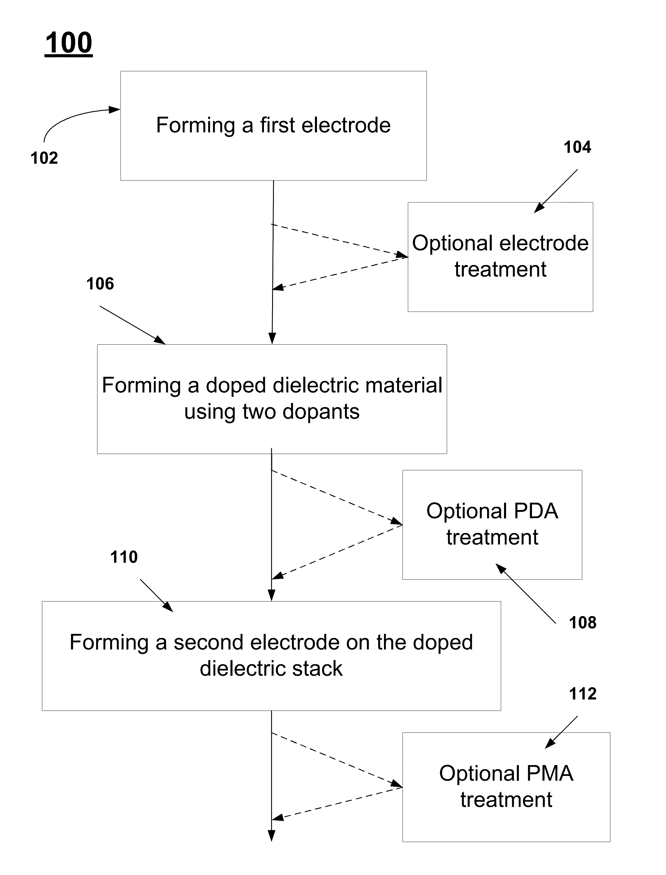
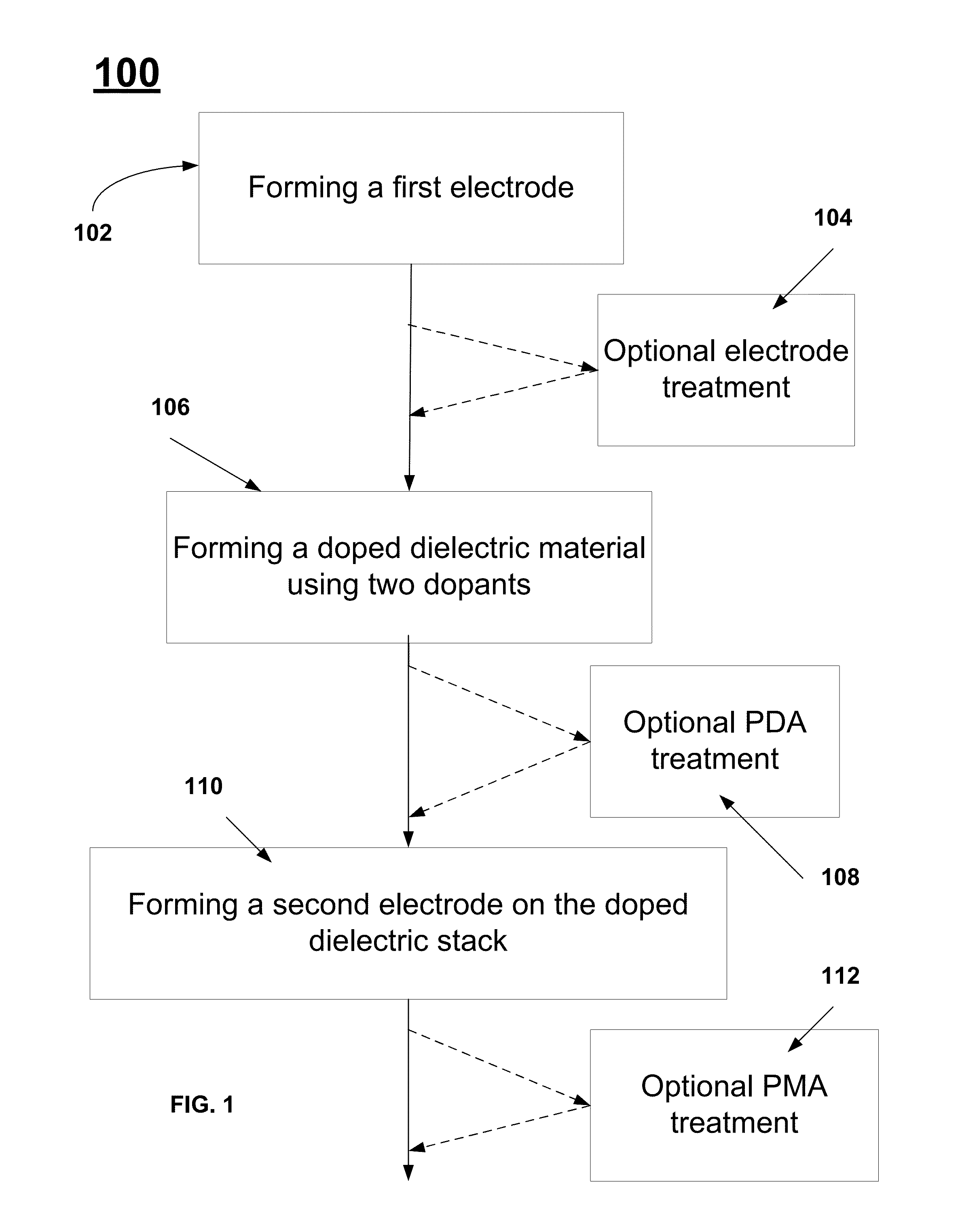
[0013]In some embodiments of the present invention, a first dopant is added to the dielectric material to decrease the leakage current in MIM DRAM capacitors. Advantageously, the first dopant is selected to have an ionic radius that is smaller than that of the metal atom in the base dielectric material. A second dopant which has an ionic radius that is larger in size than that of the first dopant is also added to the dielectric material to further reduce the leakage current by adding additional carrier compensation capacity and by relieving the strain on the dielectric matrix induced by the first dopant and increase the polarization of the high k dielectric matrix. This may also have the benefit of reducing the EOT. Advantageously, the second dopant is selected to have an ionic radius that is larger than that of the metal atom in the base dielectric material. In some embodiments of the present invention, the dielectric material is TiO2, the first dopant is one of Al or Ge, and the second dopant is one of Ga, Y, La, Zr, Hf, Sc, Nd, Ce, In, Sn, Er, Gd, Mg, Mn, Lu, Pr, or Co. In some embodiments of the present invention, the second dopant is chosen to fill the oxygen vacancies and substitute for the oxygen atoms in the matrix. Examples of this type of dopants comprise one of S, Se, Te, C, F, Cl, Br, I, P, As, Sb, and Bi.

Problems solved by technology

The low band gap may lead to high leakage current in the device.
As a result, without the utilization of countervailing measures, capacitor stacks implementing high-k dielectric materials may experience large leakage currents.
The noble metal systems, however, are prohibitively expensive when employed in a mass production context.
Moreover, electrodes fabricated from noble metals often suffer from poor manufacturing qualities, such as surface roughness, poor adhesion, and form a contamination risk in the fab.
High k metal oxide materials generally possess a number of defects in the form of oxygen vacancies.
Annealing the dielectric material in an oxidizing atmosphere after deposition will improve the leakage current; however, oxygen vacancies will still be present.
However, Al and Ge are small atoms, have limited solubility in TiO2, and their incorporation distorts the TiO2 matrix.

Method used


Image

  • Doping approach of titanium dioxide for dram capacitors
  • Doping approach of titanium dioxide for dram capacitors
  • Doping approach of titanium dioxide for dram capacitors

Examples


Embodiment Construction

[0021]A detailed description of one or more embodiments is provided below along with accompanying figures. The detailed description is provided in connection with such embodiments, but is not limited to any particular example. The scope is limited only by the claims and numerous alternatives, modifications, and equivalents are encompassed. Numerous specific details are set forth in the following description in order to provide a thorough understanding. These details are provided for the purpose of example and the described techniques may be practiced according to the claims without some or all of these specific details. For the purpose of clarity, technical material that is known in the technical fields related to the embodiments has not been described in detail to avoid unnecessarily obscuring the description.

[0022]The dielectric constant of a dielectric material may be dependent upon the crystalline phase(s) of the material. For example, in the case of TiO2, the anatase crystallin...


PUM

PropertyMeasurementUnit
cell capacitanceaaaaaaaaaa
physical thicknessaaaaaaaaaa

Abstract

A method for fabricating a DRAM capacitor stack is described wherein the dielectric material is a doped material formed from a first dopant in concert with a second dopant wherein the second dopant has a different physical size from the first dopant and the presence of the second dopant influences the solubility of the first dopant in the dielectric material. The dielectric material maintains a high k-value while minimizing the leakage current and the EOT value

Description

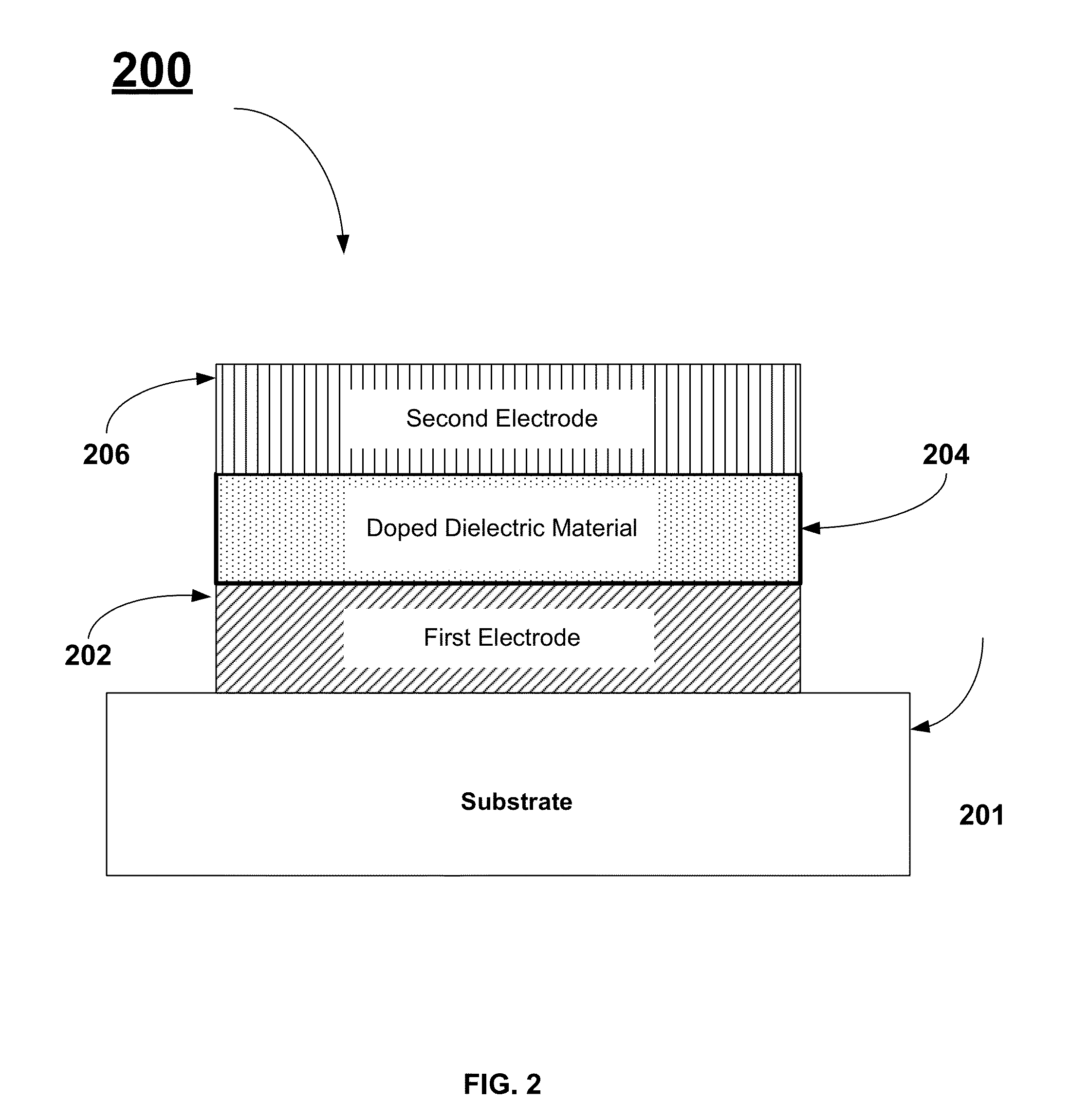
[0001]This document relates to the subject matter of a joint research agreement between Intermolecular, Inc. and Elpida Memory, Inc.FIELD OF THE INVENTION[0002]The present invention generally relates to the field of dynamic random access memory (DRAM), and more particularly to dielectric material processing for improved DRAM performance.BACKGROUND OF THE INVENTION[0003]Dynamic Random Access Memory utilizes capacitors to store bits of information within an integrated circuit. A capacitor is formed by placing a dielectric material between two electrodes formed from conductive materials. A capacitor's ability to hold electrical charge (i.e., capacitance) is a function of the surface area of the capacitor plates A, the distance between the capacitor plates d (i.e. the physical thickness of the dielectric layer), and the relative dielectric constant or k-value of the dielectric material. The capacitance is given by:C=κɛoAd(Eqn.1)where ∈0 represents the vacuum permittivity.[0004]The diele...

Claims


Application Information

Patent Timeline
Patent Type & Authority Applications(United States)
IPC IPC(8): H01L21/02
CPCH01L28/40
Inventor DEWEERD, WIMCHEN, HANHONGODE, HIROYUKI
Owner INTERMOLECULAR
Why Eureka
Try Eureka