Elongated bump structure in semiconductor device

a semiconductor device and bump structure technology, applied in semiconductor devices, semiconductor/solid-state device details, electrical devices, etc., can solve the problems of limiting the pitch dimension of metal trace lines for interconnections, current circular shaped bumps will eventually become bottlenecks to continuous device shrinkage, and mechanical stress created at packaging circuitry as well as the underlying layers

Active Publication Date: 2013-03-14
TAIWAN SEMICON MFG CO LTD
View PDF17 Cites 62 Cited by
  • Summary
  • Abstract
  • Description
  • Claims
  • Application Information

AI Technical Summary

Benefits of technology

[0002]Integrated circuit chips comprise semiconductor devices formed on a substrate such as a semiconductor wafer and include metalized contact, or attachment, pads for providing an electrical interface to the integrated circuitry. Conventional techniques for providing a connection between the internal circuitry of a chip and external circuitry, such as a circuit board, another chip, or a wafer, include wire bonding, in which wires are used to connect the chip contact pads to the external circuitry, and may also include other techniques known in the art. A more recent chip connection technique, known as flip chip technology, provides for connection of integrated circuit devices to external circuitry using solder bumps that have been deposited onto the chip contact pads. In order to mount the chip to external circuitry, the chip is flipped over so that its top side faces down and its contact pads are aligned with matching contact pads on the external circuit. The solder is then flowed between the flipped chip and the substrate supporting the external circuitry to complete the interconnect. The resulting flip chip package is much smaller than a traditional carrier-based system, because the chip is positioned directly on the external circuitry, such that the interconnect wires may be much shorter. As a result, the inductance and resistive heat are greatly reduced, enabling higher-speed devices.

Problems solved by technology

For example, circular shaped copper pillar bumps add significant size to the interconnect structure, thereby limiting the pitch dimension of metal trace lines for the interconnect.
As a result, the current circular shaped bumps will eventually become a bottleneck to the continuous device shrinking in the integrated circuit (IC) industry.
Another disadvantage to circular copper pillar bumps is the mechanical stress created at the packaging circuitry as well as the underlying layers due to mismatched thermal expansion of the chip and the packaging structure.
The packaging structure therefore becomes more and more fragile.
In addition, the large electrical current density at the circular bump-to-pad interface contributes to electromigration and electric stress.

Method used


Image

  • Elongated bump structure in semiconductor device
  • Elongated bump structure in semiconductor device
  • Elongated bump structure in semiconductor device

Examples


Embodiment Construction

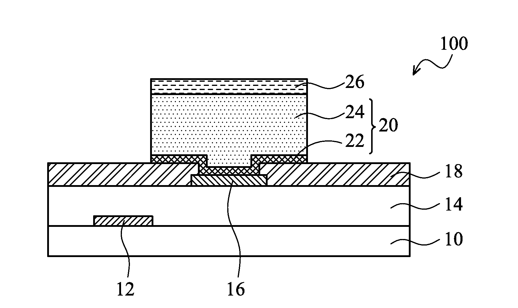
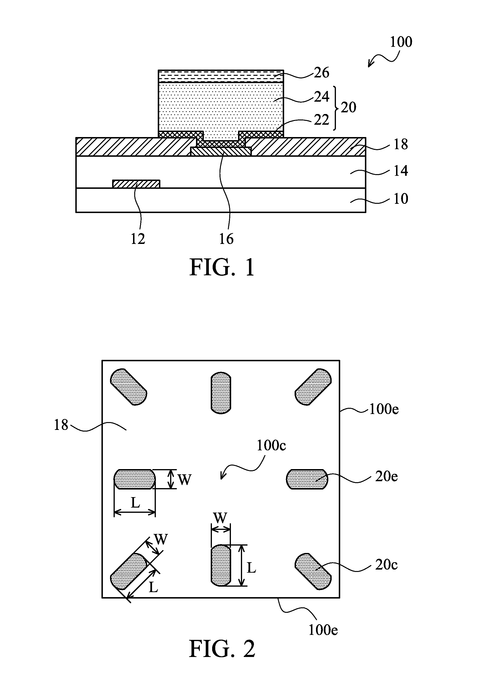
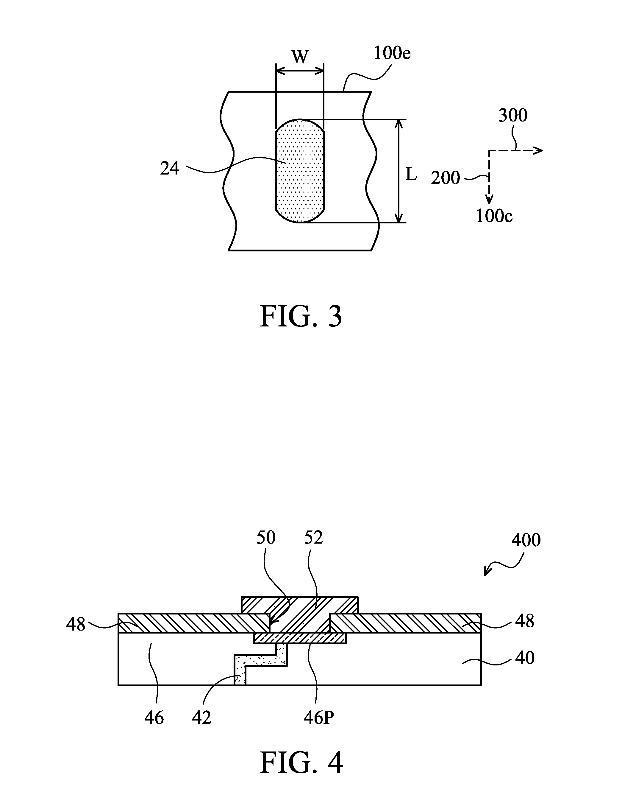
[0010]The making and using of the embodiments of the disclosure are discussed in detail below. It should be appreciated, however, that the embodiments provide many applicable inventive concepts that can be embodied in a wide variety of specific contexts. The specific embodiments discussed are merely illustrative of specific ways to make and use the embodiments, and do not limit the scope of the disclosure. Embodiments described herein relate to the use of elongated bump structures for use with semiconductor devices. As will be discussed below, embodiments are disclosed that utilize an elongated bump structure for the purpose of attaching one substrate to another substrate, wherein each substrate may be a die, wafer, interposer substrate, printed circuit board, packaging substrate, or the like, thereby allowing for die-to-die, wafer-to-die, wafer-to-wafer, die or wafer to interposer substrate or printed circuit board or packaging substrate, or the like. Throughout the various views a...


PUM


Abstract

A device includes a chip attached to a substrate. The chip includes a conductive pillar having a length (L) measured along a long axis of the conductive pillar and a width (W) measured along a short axis of the conductive pillar. The substrate includes a conductive trace and a mask layer overlying the conductive trace, wherein the mask layer has an opening exposing a portion of the conductive trace. An interconnection is formed between the conductive pillar and the exposed portion of the conductive trace. The opening has a first dimension (d1) measured along the long axis of the conductive pillar and a second dimension (d2) measured along the short axis of the conductive pillar. A ratio of L to d1 is greater than a ratio of W to d2.

Description

TECHNICAL FIELD[0001]This disclosure relates to semiconductor devices, and more particularly, to an elongated bump structure in a semiconductor device and a package assembly.BACKGROUND[0002]Integrated circuit chips comprise semiconductor devices formed on a substrate such as a semiconductor wafer and include metalized contact, or attachment, pads for providing an electrical interface to the integrated circuitry. Conventional techniques for providing a connection between the internal circuitry of a chip and external circuitry, such as a circuit board, another chip, or a wafer, include wire bonding, in which wires are used to connect the chip contact pads to the external circuitry, and may also include other techniques known in the art. A more recent chip connection technique, known as flip chip technology, provides for connection of integrated circuit devices to external circuitry using solder bumps that have been deposited onto the chip contact pads. In order to mount the chip to ex...

Claims


Application Information

Patent Timeline
Patent Type & Authority Applications(United States)
IPC IPC(8): H01L23/485
CPCH01L24/11H01L2924/00014H01L24/14H01L2224/05611H01L2224/05644H01L2224/05647H01L2224/05655H01L2224/05671H01L2224/1145H01L2224/11452H01L2224/11462H01L2224/13013H01L2224/13082H01L2224/13083H01L2224/13109H01L2224/13111H01L2224/1312H01L2224/13139H01L2224/13144H01L2224/13147H01L2224/13155H01L2224/13164H01L2224/13169H01L2224/141H01L2224/16145H01L2224/16225H01L2224/81193H01L2224/81815H01L2224/14135H01L2224/05572H01L2224/13005H01L2224/16059H01L24/16H01L2224/0345H01L2224/05026H01L2224/05166H01L2224/05181H01L2224/05186H01L2924/13091H01L2924/01012H01L2924/01029H01L2224/0401H01L2924/1306H01L2924/1305H01L24/13H01L2924/04941H01L2924/04953H01L2924/01013H01L2924/01073H01L2924/01049H01L2924/0105H01L2924/0103H01L2924/01025H01L2924/01024H01L2924/01022H01L2924/01032H01L2924/01038H01L2924/01078H01L2924/0104H01L2924/206H01L2924/01082H01L2924/01046H01L2924/01079H01L2924/01047H01L2924/01083H01L2924/01051H01L2224/13012H01L2924/00012H01L2924/00H01L2224/05552H01L2224/13014H01L2224/1308H01L2224/14145
Inventor KUO, CHEN-CHENGCHUANG, CHITALIN, TSUNG-SHUCHEN, CHEN-SHIEN
Owner TAIWAN SEMICON MFG CO LTD
Why Eureka
Try Eureka