Organic light-emitting diode with enhanced efficiency

a light-emitting diode and organic technology, applied in the direction of organic semiconductor devices, solid-state devices, thermoelectric devices, etc., can solve the problems of reducing device efficiency, reducing device efficiency, and adding expense and complexity to device fabrication

Active Publication Date: 2013-03-21
NITTO DENKO CORP
View PDF8 Cites 31 Cited by
  • Summary
  • Abstract
  • Description
  • Claims
  • Application Information

AI Technical Summary

Benefits of technology

[0010]For example, some embodiments provide an organic light-emitting device comprising: a cathode, an anode, and a series of organic layers disposed between the anode and the cathode, wherein the series of organic layers comprises: a first light-emitting layer deposited between the anode and the cathode, wherein the first light-emitting layer comprises a first host material and a first emissive material; a hole-transport layer, disposed between the anode and the first light-emitting layer a second light-emitting layer disposed between the first light-emitting layer and the cathode, wherein the second light-emitting layer comprises a second host material and a second emissive material; and an electron-transport layer disposed between the second light-emitting layer and the cathode; wh

Problems solved by technology

These devices may suffer from the problems of electron leakage from the light-emitting layers through the hole-transport layer to the anode, and hole leakage from the light-emitting layers through the electron-transport layer to the cathode, thus reducing the device efficiency.
Traditionally, hole-blocking and electron-blocking layers have sometimes been used to attempt to address this problem, but the additional layers add expense and complexity to the device

Method used


Image

  • Organic light-emitting diode with enhanced efficiency
  • Organic light-emitting diode with enhanced efficiency
  • Organic light-emitting diode with enhanced efficiency

Examples


example 1

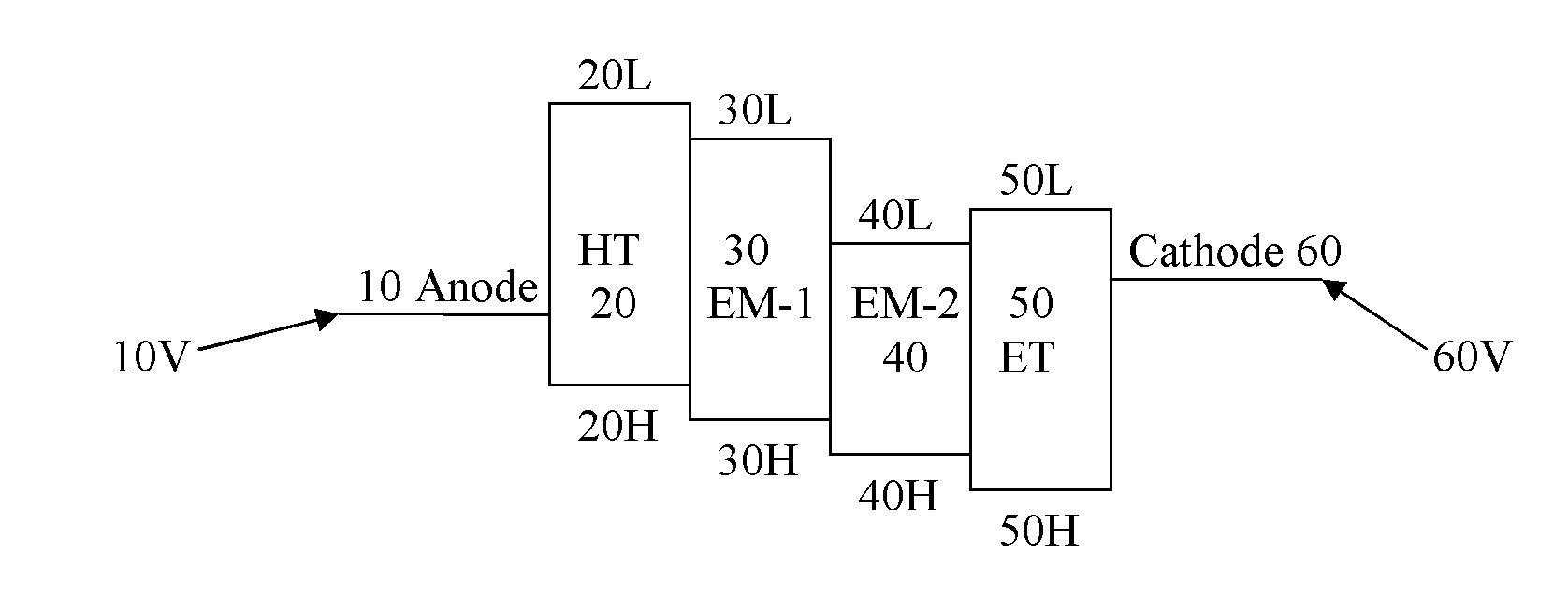
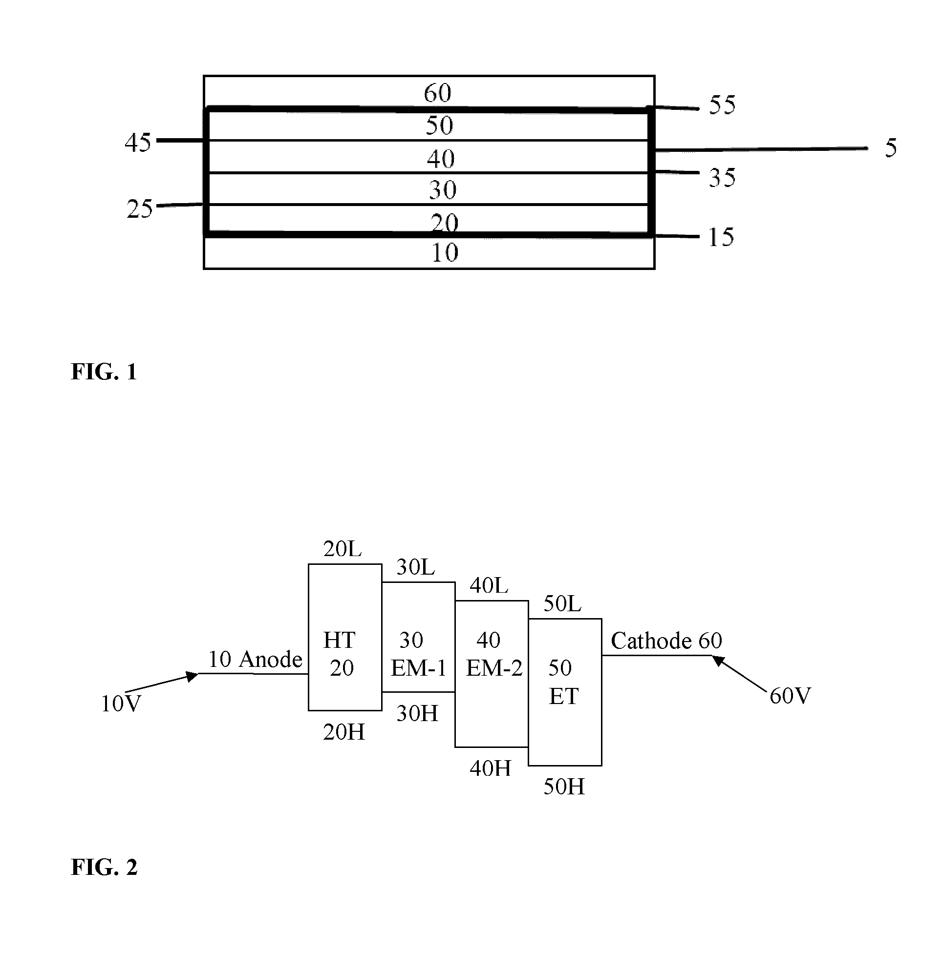
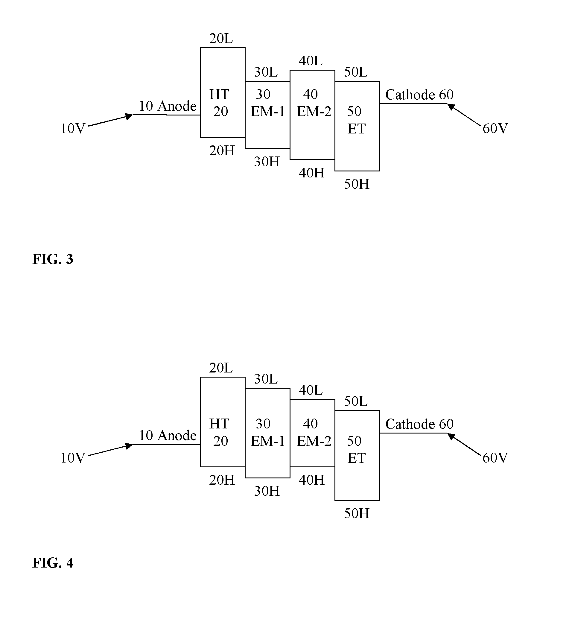
[0062]The devices were generally fabricated as follows.

[0063]ITO coated glass substrates were cleaned by ultrasound in acetone, and consecutively in 2-propanol, baked at about 110° C. for about 3 hours, followed by treatment with oxygen plasma for about 30 min. A layer of PEDOT: PSS (Baytron P from H. C. Starck) was spin-coated at about 6000 rpm onto the pre-cleaned and O2-plasma treated (ITO)-substrate and annealed at about 180° C. for about 30 min, yielding a thickness of around 20 nm. In a glove-box hosted vacuum deposition system at a pressure of about 10−7 torr (1 torr=133.322 Pa), 4,4′4″-tri(N-carbazolyl)triphenylamine (TCTA) was first deposited on top of PEDOT / PSS layer at deposition rate of about 0.06 nm / s, yielding a 40 nm thick film. Then the first emitter (about 12% wt) with the first host was co-deposited on top of TCTA to form a 5-10 nm thick film as first light-emitting layer, followed by co-deposition of the second emitter (about 5% wt) and the second host to form a 1...

example 2

[0064]The following device, which has the conventional stepwise decrease in HOMO energy levels and LUMO energy levels, was prepared according to the procedure of Example 1.

LUMOEmissiveLayerMaterial(eV)HOMO (eV)MaterialHole-transportDTASi−2.20−5.60NAFirst light-emitting4Cz-PBP−2.60−6.06FIrPicSecond light-emitting4Cz-PBP−2.60−6.06Ir(pq)2acacThird light-emitting4Cz-PBP−2.60−6.06FIrPicElectron-transportTPBI−2.70−6.20NA

[0065]The performance of this device was evaluated by I-V measurements using a Keithley 2400 Source Meter to apply 0-10 V voltage scans and measure the current simultaneously. All device operations were done inside a nitrogen-filled glove-box. FIG. 9 is a plot of the luminance efficiency and the power efficiency of the device at varying brightness. FIG. 9 shows that the luminance efficiency generally ranges from about 28 cd / A to about 31 cd / A, and the power efficiency ranges from about 19 lm / W to about 24 lm / W, at a brightness ranging from about 200 cd / m2 to about 1,000 cd...

example 3

[0066]The following device, which has the conventional stepwise decrease in HOMO energy levels, was prepared according to the procedure of Example 1.

LUMOEmissiveLayerMaterial(eV)HOMO (eV)MaterialHole-transportDTASi−2.20−5.60NAFirst light-emittingHO-1−3.10−6.08FIrPicSecond light-emittingHO-1−3.10−6.08Ir(pq)2acacThird light-emittingHO-1−3.10−6.08FIrPicElectron-transportTPBI−2.70−6.20NA

[0067]The performance of this device was evaluated by I-V measurements using a Keithley 2400 Source Meter to apply 0-10 V voltage scans and measure the current simultaneously. All device operations were done inside a nitrogen-filled glove-box. FIG. 10 is a plot of the luminance efficiency and the power efficiency of the device at varying brightness. FIG. 10 shows that the luminance efficiency generally ranges from about 37 cd / A to about 42 cd / A, and the power efficiency ranges from about 24 lm / W to about 33 lm / W, at a brightness ranging from about 200 cd / m2 to about 1,000 cd / m2 brightness. At 1,000 cd / m2...


PUM

PropertyMeasurementUnit
Fractionaaaaaaaaaa
Wavelengthaaaaaaaaaa

Abstract

Generally, the devices provided herein comprise at least a hole-transport layer, two light-emitting layers, and an electron-transport layer, each having a highest occupied molecular orbital (HOMO) energy level and a lowest unoccupied molecular orbital (LUMO) energy level, wherein at least one of the HOMO energy levels and/or the LUMO energy levels of at least one of the light-emitting layers does not decrease in a stepwise fashion.

Description

CROSS-REFERENCE TO RELATED APPLICATIONS[0001]This application claims the benefit of U.S. Provisional Application No. 61 / 301,694, filed Feb. 5, 2010, which is incorporated by reference herein in its entirety.BACKGROUND[0002]1. Field[0003]The embodiments described herein relate to organic light-emitting diodes, such as organic light-emitting diodes comprising a hole-transport layer, two light-emitting layers, and an electron-transport layer.[0004]2. Description of the Related Art[0005]White organic light emitting devices (WOLED) are becoming increasingly important for lighting applications. For example, WOLEDs may be able to replace fluorescent tubes to save energy. Thus there is a continuing need to improving the power efficiency of WOLEDs.[0006]Many of the current WOLEDs comprise a hole-transport layer, at least two light-emitting layers, and an electron-transport layer arranged in that order. In these devices, each layer has a highest occupied molecular orbital (HOMO) energy level ...

Claims


Application Information

Patent Timeline
IPC IPC(8): H01L51/54
CPCH01L51/0037H01L51/0059H01L51/0062H01L2251/552H01L51/0094H01L51/5016H01L51/5036H01L51/0067H10K85/1135H10K85/649H10K85/631H10K85/654H10K85/40H10K50/125H10K50/11H10K2101/10H10K2101/30H10K50/13H10K85/342H10K50/15H10K50/16
Inventor MA, LIPING
Owner NITTO DENKO CORP
Why Eureka
Try Eureka