Method for Predicting Reliable Lifetime of SOI Mosfet Device

a technology of soi mosfet and reliable lifetime, which is applied in the field of reliable lifetime prediction of soi mosfet devices, can solve the problems of time dependent dielectric breakdown, inability to scale down various reliability problems in proportion, and inability to accurately predict the effect of the operation voltag

Inactive Publication Date: 2013-04-25
PEKING UNIV
View PDF2 Cites 13 Cited by
  • Summary
  • Abstract
  • Description
  • Claims
  • Application Information

AI Technical Summary

Benefits of technology

[0026]Compared with the conventional method for testing the lifetime of the SOI MOSFET device, the method provided by embodiments of the invention prevents a self-heating effect from affecting the prediction of a lifetime of a SOI MOSFET device in a practical logic circuit or in an AC analog circuit, which leads to a more precise prediction result.

Problems solved by technology

However, the operation voltage is not able to be scaled down in a proportion while the size of the device is scaled down.
Therefore, various reliability problems are gradually becoming more serious, mainly including the hot carrier effect (HCI), the negative bias thermal instability (NBTI) and an time dependent dielectric breakdown (TDDB), etc.
However, due to the quite lower thermal conductivity of buried oxide layer in the SOI MOSFET device, the lattice temperature of a channel region in the device rises, resulting in a decrease of the on-state drain current of the device.
However, an error may occurr when predicting a logic circuit or an AC analog circuit operated in real world by the method.
More specifically, if the operating frequency is higher, the thermal response of the device is conducted so soon that a signal has not been built yet.
Meanwhile, if the operating frequency is lower, the self-heating effect is getting more serious.

Method used


Image

  • Method for Predicting Reliable Lifetime of SOI Mosfet Device
  • Method for Predicting Reliable Lifetime of SOI Mosfet Device
  • Method for Predicting Reliable Lifetime of SOI Mosfet Device

Examples


Embodiment Construction

[0036]A preferred embodiment of the invention will be described in more detail with reference to the accompany drawings.

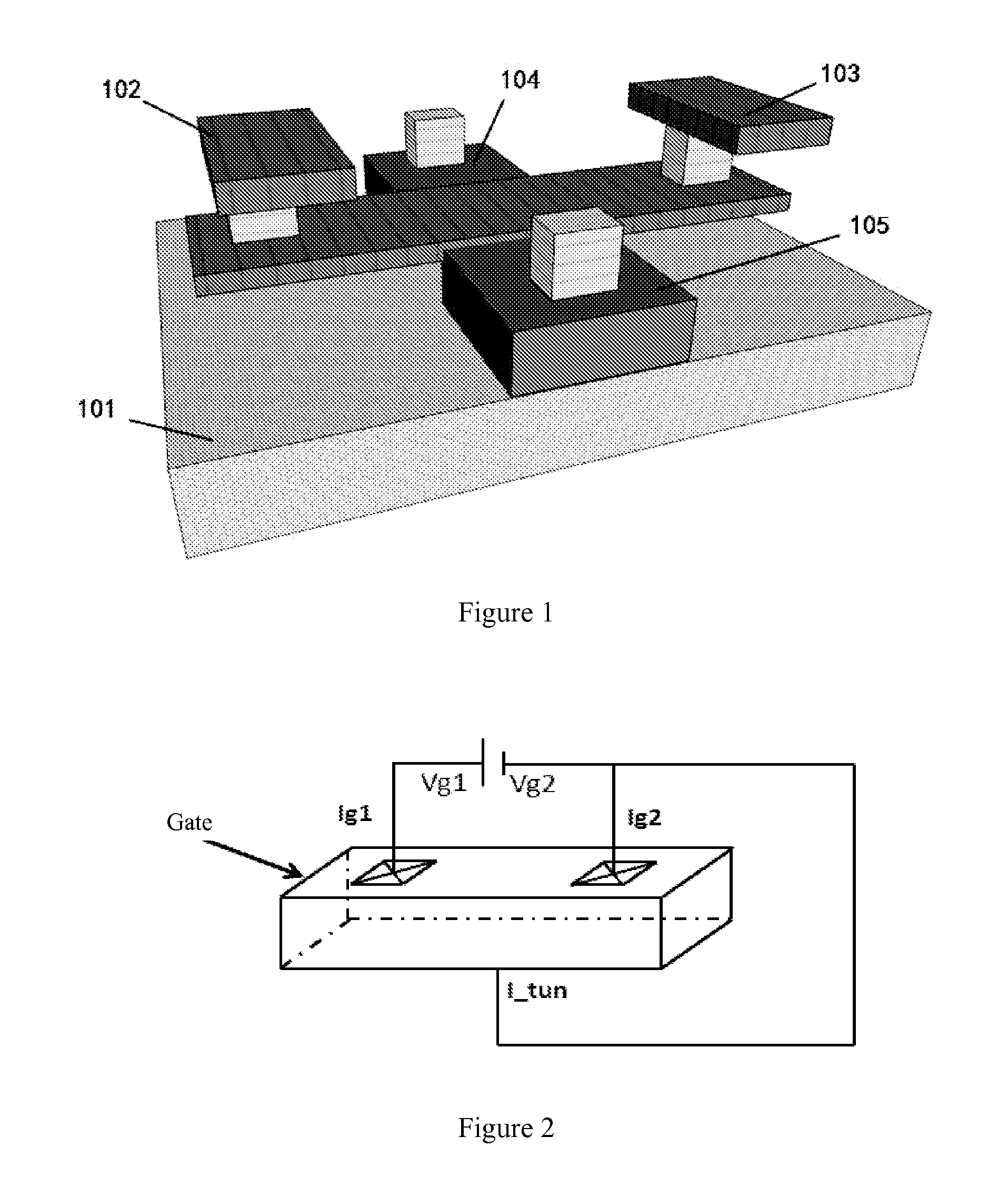
[0037]In the embodiment, a SOI MOSFET device to be tested is a SOI NMOS device (a PMOS device is similar to it) having body contacts at five terminals, and a three-dimensional schematic view thereof is shown in FIG. 1. An NMOS transistor having a good process condition and a uniform interface state is selected. The width (W) and the length (L) of the device are 5 μm and 0.18 μm, respectively. The specific implementation steps are as follows.

[0038]1) The gate resistances under different wafer temperatures and stress biases are extracted. The method is described as follows. As shown in FIG. 2, a gate 1 and a gate 2 are applied with a voltage Vg1 and a voltage Vg2, respectively. In order to avoid the influence from the gate tunneling current on the detection of a current Ig1 and a current Ig2, the voltages Vg1 and Vg2 are set as Vg1=Vg+ΔVg and Vg2=Vg−ΔVg, where Vg is ...


PUM


Abstract

Disclosed herein is a method for predicting a reliable lifetime of a SOI MOSFET device. The method comprises: measuring a relationship of a gate resistance of the SOI MOSFET device varying as a function of a temperature at different wafer temperatures; performing a lifetime accelerating test on the SOI MOSFET device at different wafer temperatures, so as to obtain a degenerating relationship of a parameter representing the lifetime of the device as a function of stress time, and obtain a lifetime in the presence of self-heating when the parameter degenerates to 10%; performing a self-heating correction on the measured lifetime of the device by using the measured self-heating temperature and an Arrhenius model, so as to obtain a lifetime without self-heating influence; performing a self-heating correction on a variation of the drain current caused by self-heating; performing a self-heating correction on an impact ionization rate caused by hot carriers; and predicting the lifetime of the SOI MOSFET device under a bias. The embodiment of the invention prevents the self-heating effect from affecting the SOI MOSFET device in a practical logic circuit or in an AC analog circuit, which leads to a more precise prediction result.

Description

FIELD OF THE INVENTION[0001]An embodiment of the invention relates to the technical field of semiconductor reliability. Since the self-heating effect of a SOI MOSFET device exacerbates the degradation degree of the device, while in a practical digital circuit the influence of the self-heating effect is very small, the embodiment of the invention mainly relates to a method for predicting a reliable lifetime of the SOI MOSFET device after a self-heating correction.BACKGROUND OF THE INVENTION[0002]With a rapid development of Very Large Scale Integrated circuits (VLSI) technology, the silicon integrated circuit process has entered a product manufacturing stage generally based on a feature size of deep submicron and even to ultra-deep submicron. The progress of fabrication process greatly increases quality and performance of VLSI while dramatically reduces the process cost of an individual chip, thus promotes the product popularization of integrated circuit and brings a new electronic in...

Claims


Application Information

Patent Timeline
Patent Type & Authority Applications(United States)
IPC IPC(8): G01R31/26G06F19/00
CPCG01R31/287
Inventor HUANG, RUYANG, DONGAN, XIAZHANG, XING
Owner PEKING UNIV
Why Eureka
Try Eureka