Method to form solder deposits and non-melting bump structures on substrates

a technology of substrates and bump structures, applied in the direction of printed circuit manufacturing, basic electric elements, electric apparatus, etc., can solve the problems of requiring various patterning steps, silicon chip and organic board structure has experienced an obvious explosive growth, and the flip chip device mounted on a low-cost organic circuit board has experienced a dramatic growth

Inactive Publication Date: 2013-05-02
ATOTECH DEUT GMBH
View PDF7 Cites 35 Cited by
  • Summary
  • Abstract
  • Description
  • Claims
  • Application Information

AI Technical Summary

Benefits of technology

[0009]It is therefore an objective of the present invention to adopt an electroplating method of tin and tin alloys to produce a uniform layer of a solder deposit on a substrate and a tin plating bath composition suitable therefore. Such plating methods should be suitable to fill recess structures possessing high aspect ratios without leaving voids or dimples.
[0011]Another object of the present invention is to provide a method for solder deposition and formation of non-melting bump structures having a reduced number of plating steps and which is universally applicable even when the solder resist openings have different dimensions.
[0012]Another object of the present invention is to provide a method for solder deposit and non-melting bump structure formation which avoids pattern misalignment.

Problems solved by technology

However, in recent years, driven by the demand of high-density, high-speed and low-cost semiconductor devices for the trend of miniaturization of modern electronic products, the flip chip devices mounted on a low-cost organic circuit board (e.g. printed circuit board or substrate) with an epoxy underfill to mitigate the thermal stress induced by the thermal expansion mismatch between the silicon chip and organic board structure have experienced an obviously explosive growth.
Although electroplate solder bumping on the circuit board offers finer bump pitch over stencil printing, it presents several challenges for initial implementation.
To apply this method various patterning steps are required which is not desired from the overall standpoint of process efficiency.
Each patterning step is a potential cause of mismatched patterns.
Furthermore the method has its limitations if the distance between adjacent contact areas (pitch) is very small as a result of the miniaturization of electronic devices.
This method can lead to a misalignment of the individually patterned solder resin layer and additional resin layer in case of small contact area size and narrow pitch distance.

Method used


Image

  • Method to form solder deposits and non-melting bump structures on substrates
  • Method to form solder deposits and non-melting bump structures on substrates
  • Method to form solder deposits and non-melting bump structures on substrates

Examples


example 1

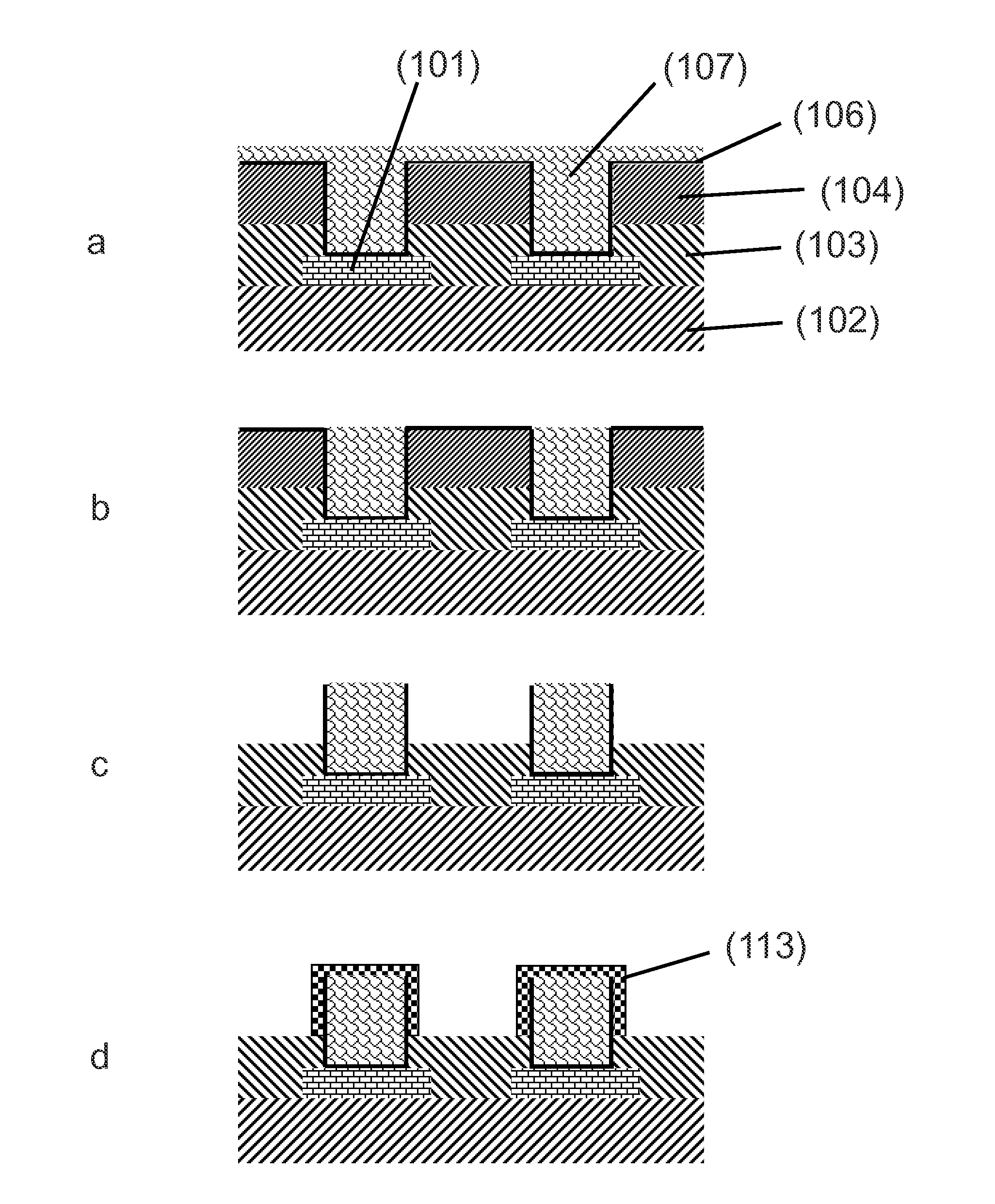
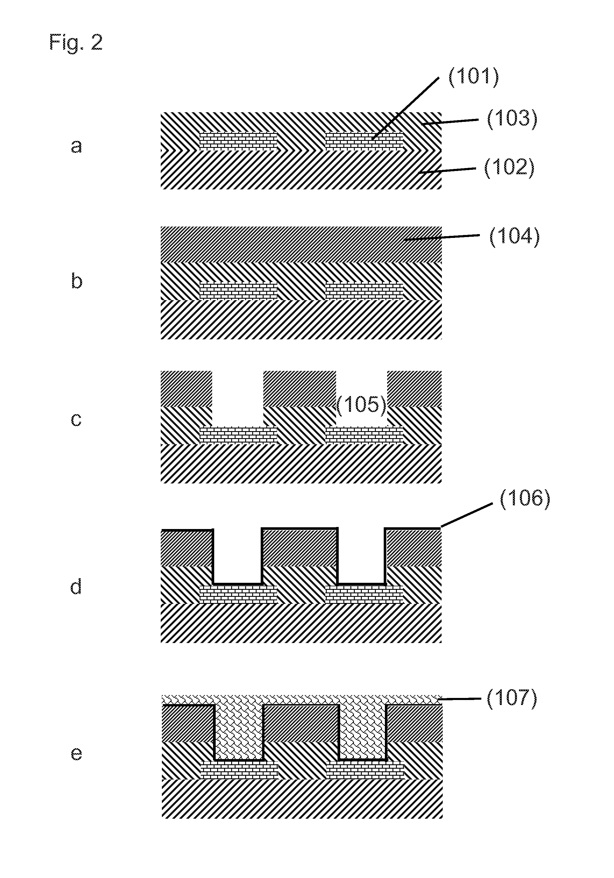
[0154]An IC substrate is used having a contact pad structure according to FIG. 2a.

[0155]The non-conductive substrate (102) consists of GX-13 material (manufacturer: Ajinomoto Fine-Techno Co., Inc.), the permanent resin layer (103) consists of GX-92 material (manufacturer: Ajinomoto Fine-Techno Co., Inc., height of the layer: 25 μm) and the contact pads consist of copper.

[0156]A temporary resin layer (104) (DuPont PM 200, height: 50 μm) was laminated onto the permanent resin layer (103).

[0157]Next, contact area openings (105) are formed through the temporary resin layer (104) and the permanent resin layer (103) with a UV laser in one step. The diameter of the contact area openings (105) is 100 μm.

[0158]The plating sequence is according to FIG. 2d to e. First, a first conductive seed layer (106) of copper is formed on the entire substrate surface. For this the surface is first contacted with an acidic solution containing ionogenic palladium and then with a solution for electroless co...

example 2

[0165]A non-melting bump structure (112) consisting of a tin-copper alloy with a solderable cap layer (113) made of tin was manufactured. An IC substrate is used having at least one contact area structure according to FIG. 2a.

[0166]The non-conducting substrate (102) consists of GX-13 material (manufacturer: Ajinomoto Fine-Techno Co., Inc.), the permanent resin layer (103) consists of GX-92 material (manufacturer: Ajinomoto Fine-Techno Co., Inc., height of the layer: 25 μm) and the contact pads (101) consist of copper.

[0167]A temporary resin layer (104) (DuPont PM 200, height: 50 μm) was laminated onto the permanent resin layer (103).

[0168]Next, contact area openings (105) are formed through the temporary resin layer (104) and the permanent resin layer (103) with a UV laser in one step. The diameter of the contact area openings (105) is 100 μm.

[0169]The plating sequence is according to FIG. 2d to e. A first conductive seed layer (106) of copper is formed on the entire substrate surf...

example 3

[0177]A non-melting bump structure (112) consisting of copper with a solderable cap layer (113) made of tin was manufactured.

[0178]An IC substrate comprising a non-conductive substrate (102), contact areas (101), a permanent resin layer (103) and a temporary resin layer (104) as used in Example 1 is provided.

[0179]Contact area openings (105) are formed through the temporary resin layer (104) and the permanent resin layer (103) with a UV laser in one step. The diameter of the contact area openings (105) is 100 μm. The plating sequence is according to FIG. 2d to e. A first conductive seed layer (106) of copper is formed on the entire substrate surface. For this the surface is first contacted with an acidic solution containing ionogenic palladium and then with a solution for electroless copper deposition.

[0180]Thereafter, a copper layer (107) is electroplated onto the first conductive seed layer (106) from a bath containing: 45 g / l Cu2+ as CuSO4, 50 ml / l H2SO4, 1 ml / l brightener and 20...


PUM

PropertyMeasurementUnit
Tgaaaaaaaaaa
Tgaaaaaaaaaa
Tgaaaaaaaaaa

Abstract

Described is a method of forming a metal or metal alloy layer onto a substrate comprising the following steps i) provide a substrate including a permanent resin layer on top of at least one contact area and a temporary resin layer on top of the permanent resin layer, ii) contact the entire substrate area including the at least one contact area with a solution suitable to provide a conductive layer on the substrate surface and i) electroplate a metal or metal alloy layer onto the conductive layer.

Description

FIELD OF THE DISCLOSURE[0001]The invention relates to the formation of solder deposits by electroplating, particularly to flip chip packages, more particularly to flip chip joints and board to board solder joints formed by electroplated metal or metal alloys.BACKGROUND OF THE INVENTION[0002]Since the introduction of the flip chip technology by IBM in the early 1960s, the flip chip devices have been mounted on an expensive ceramic substrate where the thermal expansion mismatch between the silicon chip and the ceramic substrate is less critical. In comparison with wire bonding technology, the flip chip technology is better able to offer higher packaging density (lower device profile) and higher electrical performance (shorter possible leads and lower inductance). On this basis, the flip chip technology has been industrially practiced for the past 40 years using high-temperature solder (controlled-collapse chip connection, C4) on ceramic substrates. However, in recent years, driven by ...

Claims


Application Information

Patent Timeline
Patent Type & Authority Applications(United States)
IPC IPC(8): H05K3/40
CPCH01L21/4853H01L23/49816H01L24/13H01L2224/11474H01L2224/1148H01L2224/81192H01L2924/01004H01L2924/01012H01L2924/01013H01L2924/01025H01L2924/01029H01L2924/0103H01L2924/01032H01L2924/01038H01L2924/01049H01L2924/01051H01L2924/01052H01L2924/01056H01L2924/01061H01L2924/01079H01L2924/01082H05K3/3473H05K3/4007H05K2203/054H05K2203/0577H01L2924/014H01L2924/01005H01L2924/01006H01L2924/01019H01L2924/0102H01L2924/01023H01L2924/01024H01L2924/01042H01L2924/01044H01L2924/01045H01L2924/01047H01L2924/01074H01L2924/01075H01L2924/01077H01L2924/01078H01L24/11H01L2224/13007H01L2224/11825H01L24/05H01L2224/0346H01L2224/05567H01L2224/05573H01L2224/05644H01L2224/05647H01L2224/05655H01L2224/11462H01L2224/11849H01L2224/13022H01L2224/13082H01L2224/13083H01L2224/13111H01L2224/13139H01L2224/13144H01L2224/13147H01L2224/13155H01L2224/13164H01L2224/13171H01L2224/13562H01L2224/13611H01L2224/13166H01L2224/11906H01L2924/10253H01L2224/0401H01L2924/00014H01L2924/00H01L2224/05552H01L2924/351H01L2924/15787H01L2924/12042H01L2924/14
Inventor MATEJAT, KAI-JENSLAMPRECHT, SVENEWERT, INGOSCHOENENBERGER, CATHERINEKRESS, JURGEN
Owner ATOTECH DEUT GMBH
Why Eureka
Try Eureka