

Resist-protective film-forming composition and patterning process
a film-forming composition and resist-protective technology, applied in the direction of photosensitive material processing, basic electric elements, electric instruments, etc., can solve the problems of low resist film sensitivity, undesirable use of hexafluoroalcohol group as alkali-soluble group in the protective film, complex process, etc., to enhance the resist film sensitivity, reduce the edge roughness of the resist pattern, and enhance the contrast of acid in the protective film
Active Publication Date: 2013-06-06
SHIN ETSU CHEM IND CO LTD
View PDF15 Cites 8 Cited by
- Summary
- Abstract
- Description
- Claims
- Application Information
AI Technical Summary
Benefits of technology
The resist protective film-forming composition described in the patent prevents the resist pattern from being distrupted by airborne amine, increases the sensitivity of the resist film, improves the pattern's quality, and prevents bridges between pattern features. The composition also prevents outgassing during exposure and is easily stripped off during the development process. Additionally, the composition absorbs OOB light emitted by the EUV laser, protecting the resist film from becoming sensitive to this light.
Problems solved by technology
As such, the process is complicated.
From the standpoint of transparency, the use of a hexafluoroalcohol group as the alkali-soluble group in the protective film is undesirable because the hexafluoroalcohol group having as many as six fluorine atoms possesses strong absorption.
Method used
View moreImage
Smart ImageViewing Examples

Examples
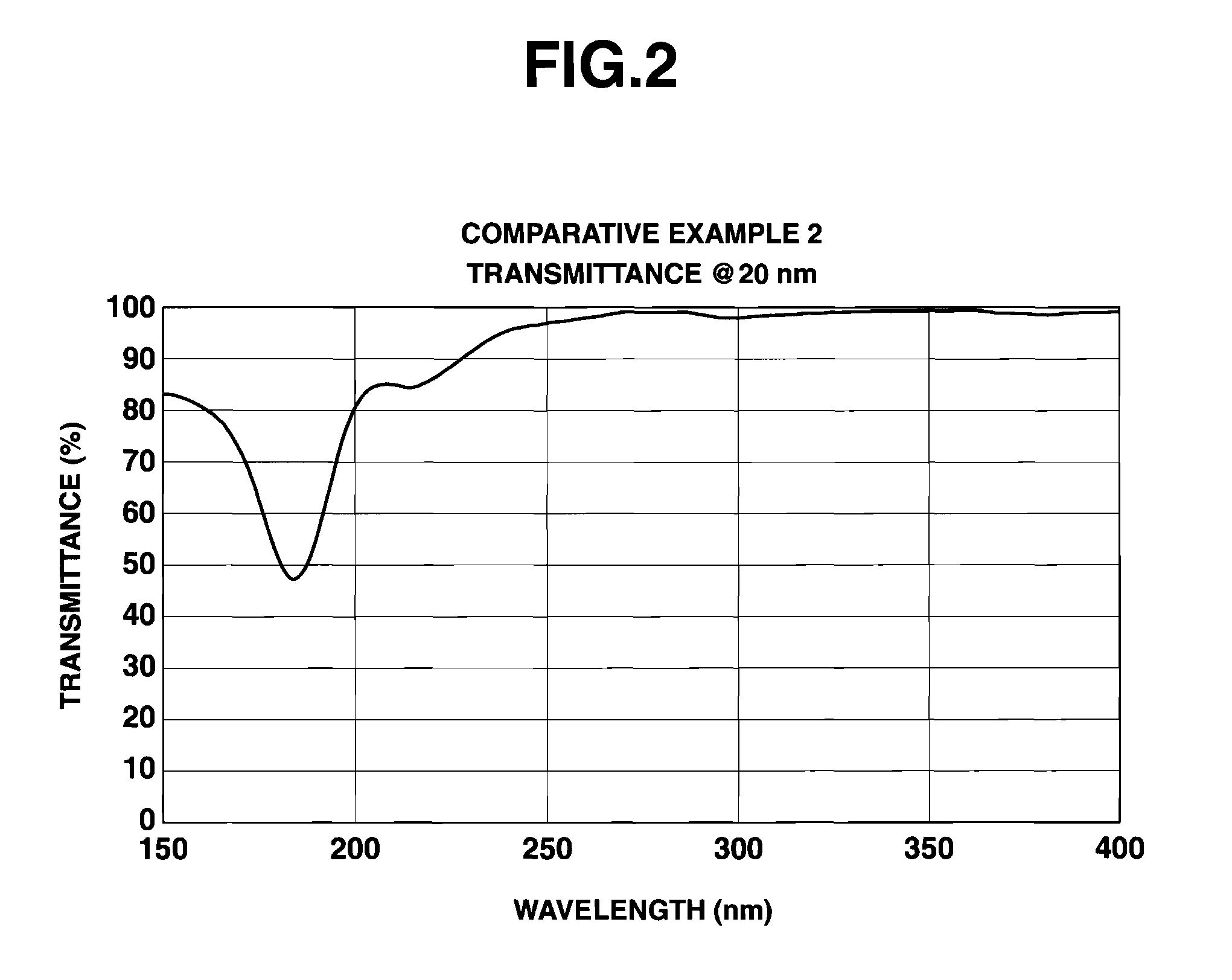
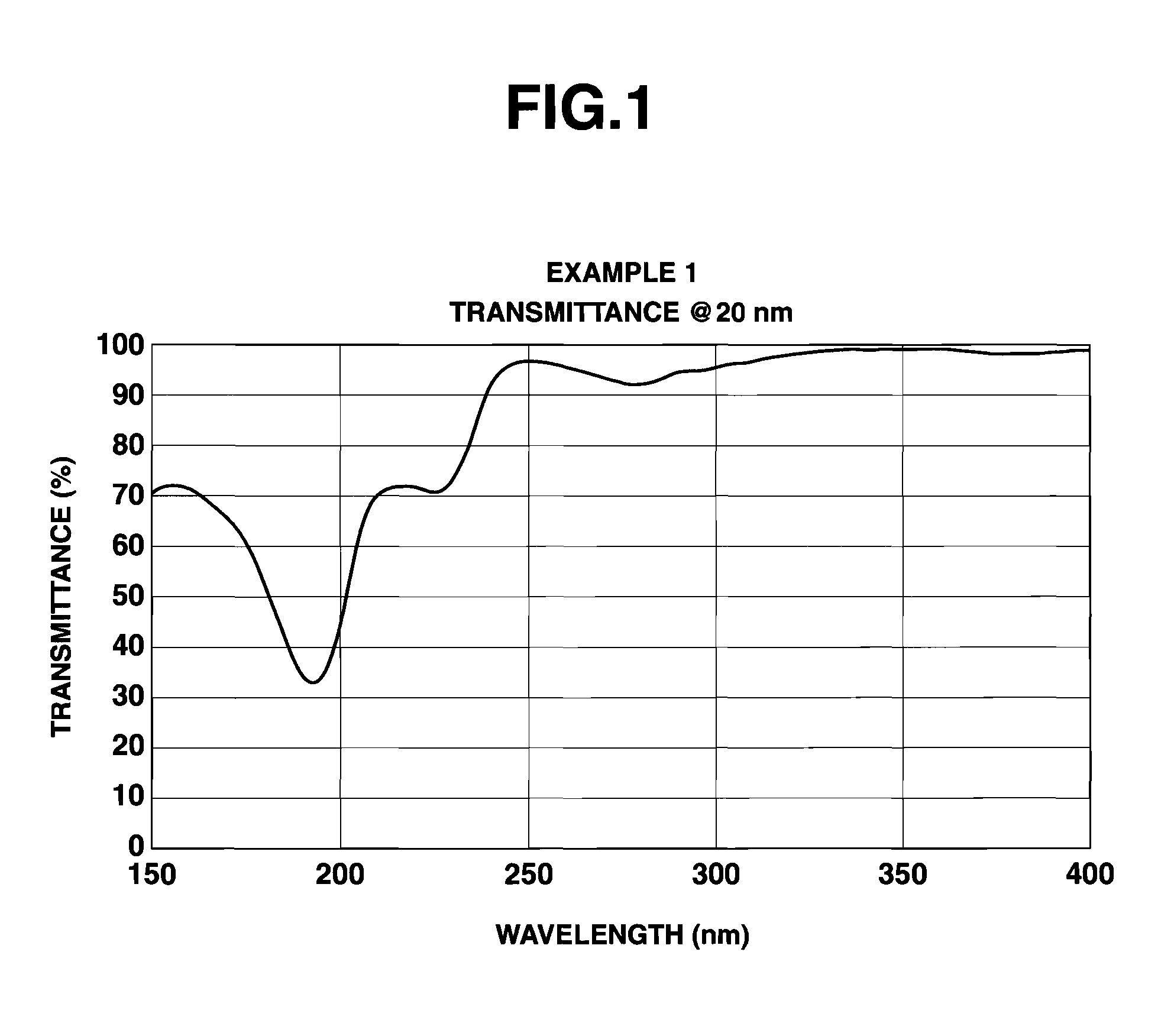
example
[0122]Examples of the invention are given below by way of illustration and not by way of limitation. It is noted that Mw and Mn are determined by GPC versus polystyrene standards using tetrahydrofuran solvent.
Login to View More PUM
| Property | Measurement | Unit |
|---|---|---|
| wavelength | aaaaa | aaaaa |
| wavelength | aaaaa | aaaaa |
| wavelength | aaaaa | aaaaa |
Abstract
A pattern is printed by forming a photoresist layer on a wafer, forming a protective film thereon, exposure, and development. The protective film is formed from a composition comprising a copolymer of hydroxystyrene with acenaphthylene and / or vinylnaphthalene and a mixture of an alcohol solvent and an ether or aromatic solvent.
Description
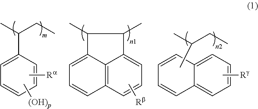
CROSS-REFERENCE TO RELATED APPLICATION[0001]This non-provisional application claims priority under 35 U.S.C. §119(a) on Patent Application Nos. 2011-266400 and 2012-121797 filed in Japan on Dec. 6, 2011 and May 29, 2012, respectively, the entire contents of which are hereby incorporated by reference.TECHNICAL FIELD[0002]This invention relates to a composition for forming a resist protective film for use in the micropatterning step in the fabrication of semiconductor devices, and a pattern forming process using the same.BACKGROUND OF THE INVENTION[0003]In the drive for higher integration and operating speeds in LSI devices, the pattern rule is made drastically finer. The rapid advance toward finer pattern rules is grounded on the development of a projection lens with an increased NA, a resist material with improved performance, and a light source with a shorter wavelength.[0004]Resist materials adapted for KrF excimer laser (248 nm) started use on the 0.3 μm process and entered the m...
Claims
Login to View More Application Information
Patent Timeline
 Patent Type & AuthorityApplications(United States)
IPC IPC(8): C09D145/00G03F7/20C09D129/02C08F232/08C08F216/10
CPCC09D145/00C08F232/08C08F216/10C09D129/02G03F7/20G03F7/11C09D125/18C08F220/283C08F220/1818G03F7/265H01L21/0273C08F220/18G03F7/26H01L21/027G03F7/32G03F7/004C08F212/24C08F220/301
InventorHATAKEYAMA, JUN
OwnerSHIN ETSU CHEM IND CO LTD