Film-forming ink, film-forming method, method of manufacturing light emitting element, light emitting element, light emitting device, and electronic apparatus

a film-forming method and film-forming technology, applied in the direction of non-metal conductors, thermoelectric devices, conductors, etc., can solve the problems of low desolvation properties, lack of preservation stability, and increase in gelation and viscosity, and achieve the effect of superior reliability

Active Publication Date: 2013-06-20
SEIKO EPSON CORP
View PDF7 Cites 14 Cited by
  • Summary
  • Abstract
  • Description
  • Claims
  • Application Information

AI Technical Summary

Benefits of technology

[0056]As a result, an electronic apparatus having superior reliability can be provided.

Problems solved by technology

However, in the film-forming ink of the related art, the aromatic hydrocarbon solvent interacts with the film-forming material to cause π-π stacking, which leads to gelation and an increase in viscosity.
Therefore, there is problem in that preservation stability is lacking.
In addition, in the film-forming ink of the related art, in addition to the interaction causing the above-described π-π stacking, since the solvent has a high boiling point, a desolvation property is low.
As a result, there is a problem in that the characteristics of the obtained organic EL element deteriorate.
When a film is formed using a liquid droplet discharge method, the above-described problems become significant because a force to prevent aggregation between π-conjugated compounds does not work unlike a spin coating method and thus the π-conjugated compounds easily aggregate.
In addition, when a light emitting layer is formed using a film-forming ink which contains a phosphorescent light emitting material formed of a metal complex, with a film-forming ink of the related art, the above-described problems relating to preservation stability and a deterioration in the characteristics of an organic EL element become significant.
The reason is considered to be that a bond between a metal of a metal complex and a ligand is unstable due to effects of dissolved oxygen and water in a solvent.
Therefore, there is a problem in that the film-forming ink does not wet and is not spread out on the hole injection layer sufficiently.
However, this configuration is not practical because the surfactant remaining in the obtained film deteriorates the characteristics of a light emitting element.

Method used


Image

  • Film-forming ink, film-forming method, method of manufacturing light emitting element, light emitting element, light emitting device, and electronic apparatus
  • Film-forming ink, film-forming method, method of manufacturing light emitting element, light emitting element, light emitting device, and electronic apparatus
  • Film-forming ink, film-forming method, method of manufacturing light emitting element, light emitting element, light emitting device, and electronic apparatus

Examples


first embodiment

Light Emitting Element

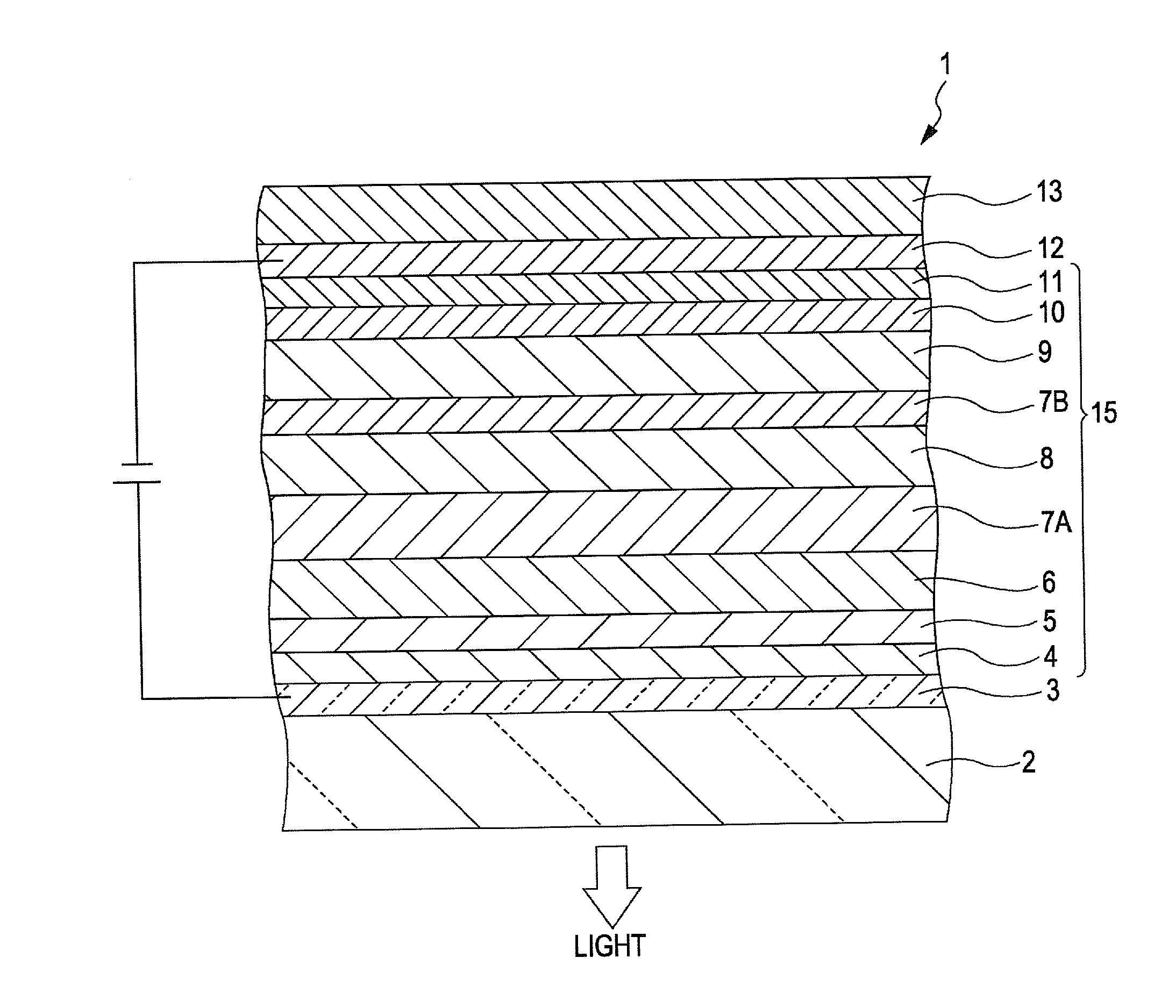
[0072]FIG. 1 is a cross-sectional view schematically illustrating a light emitting element according to an embodiment of the invention. Hereinafter, for convenience of description, the upper side and lower side of FIG. 1 are considered as “up” and “down” respectively.

[0073]A light emitting element (electroluminescence element) 1 illustrated in FIG. 1 emits red light (R), green light (G), and blue light (B) to emit white light.

[0074]In such a light emitting element 1, between an anode 3 and a cathode 12, a hole injection layer 4, a hole transport layer 5, a red-light emitting layer (first light emitting layer) 6, a first interlayer 7A, a blue-light emitting layer (second light emitting layer) 8, a second interlayer 7B, a green-light emitting layer (third light emitting layer) 9, an electron transport layer 10, and an electron injection layer 11 are laminated in this order.

[0075]In other words, the light emitting element 1 has a configuration in which a laminate ...

second embodiment

[0273]A second embodiment is different from the first embodiment in that light emitting elements are formed by elements which emit red light, green light, and blue light, respectively.

Light Emitting Device

[0274]Next, a light emitting device including light emitting elements, which are manufactured according to the method of manufacturing a light emitting element according to the embodiment, will be described with reference to FIGS. 8 and 9. FIG. 8 is a front view schematically illustrating a configuration of the light emitting device according to the embodiment, and FIG. 9 is a cross-sectional view schematically illustrating structures of major components in the light emitting device according to the embodiment.

[0275]As illustrated in FIG. 8, an organic EL device 240 according to the embodiment includes an element substrate 201 which includes three colors (R (red), G (green), and B (Blue)) of light emitting pixels 207, and a sealing substrate 202 which is disposed facing the element...

example 1

[0387] First, a transparent glass substrate having an average thickness of 0.5 mm was prepared. Next, an ITO electrode (anode) having an average thickness of 100 nm was formed on the substrate with a sputtering method.

[0388]Then, the substrate was dipped in acetone and 2-propanol in this order, followed by washing with ultrasonic waves and oxygen plasma treatment.

[0389] Next, a hole injection layer having an average thickness of 50 nm was formed on the ITO electrode.

[0390]This hole injection layer was formed by applying a hole-injection-layer-forming ink onto the ITO electrode with a liquid droplet discharge method and performing drying in a vacuum and heating (calcination) at 150° C. for 30 minutes in a nitrogen atmosphere.

[0391]For the preparation of the hole-injection-layer-forming ink, PEDOT / PSS (1 / 20) was used as the film-forming material; and a mixed dispersion medium, which included polystyrene sulfonic acid, 3,4-polyethylenedioxythiophene as a polythiophene derivative, and w...


PUM

PropertyMeasurementUnit
thicknessaaaaaaaaaa
thicknessaaaaaaaaaa
thicknessaaaaaaaaaa

Abstract

A film-forming ink according to an embodiment of the invention includes a film-forming material; and a liquid medium which dissolves or disperses the film-forming material, in which the liquid medium contains an ether compound represented by Formula (I).

Description

BACKGROUND[0001]1. Technical Field[0002]The present invention relates to a film-forming ink, a film-forming method, a method of manufacturing a light emitting element, a light emitting element, a light emitting device, and an electronic apparatus.[0003]2. Related Art[0004]Organic electroluminescence elements (organic EL elements) are light emitting elements having a structure in which at least one organic light emitting layer (light emitting layer) is interposed between an anode and a cathode. In such light emitting elements, by applying an electric field between a cathode and an anode, electrons are injected from the cathode and holes are injected from the anode, to a light emitting layer; the electrons and the holes are recombined in the light emitting layer to generate excitons; and when these excitons return to the ground state, the corresponding amount of energy is emitted as light.[0005]In general, in the organic EL elements, a hole injection layer is provided on a anode and a...

Claims


Application Information

Patent Timeline
Patent Type & Authority Applications(United States)
IPC IPC(8): H01L51/50H01L51/56H01L51/00
CPCH01L51/0007H01L51/50H01L51/56H01L51/0005H01L51/0037H01L2251/308H01L51/0042H01L51/0043H01L51/0085H01L51/5056H01L51/0039H10K71/15H10K71/135H10K85/146H10K85/115H10K85/151H10K85/1135H10K85/342H10K50/15H10K2102/103H10K71/00H10K59/1201H10K50/00
Inventor WATANABE, SHOTAROTAKIGUCHI, HIROSHI
Owner SEIKO EPSON CORP
Why Eureka
Try Eureka