

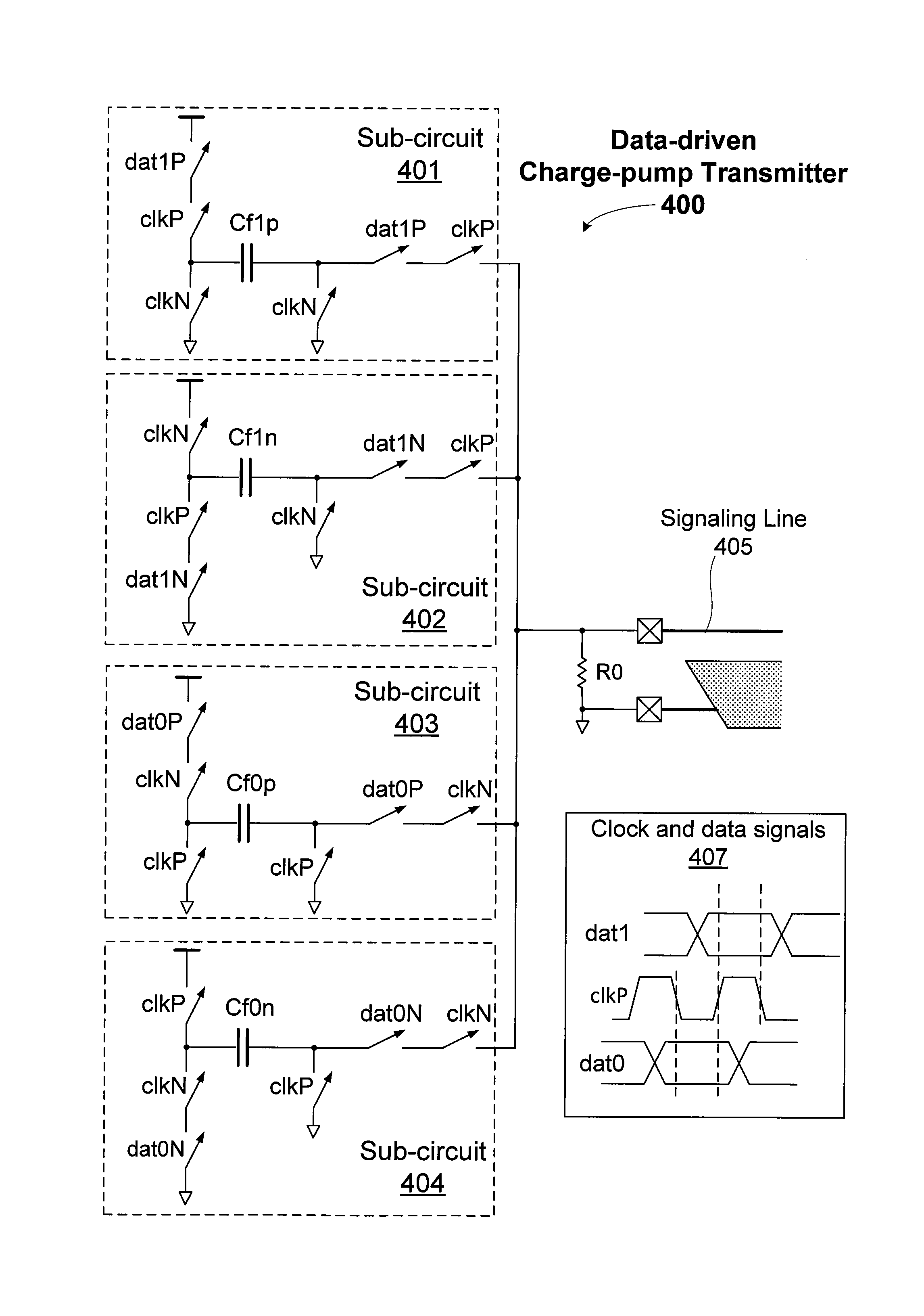
Data-driven charge-pump transmitter for differential signaling
a charge-pump transmitter and differential signaling technology, applied in the field of transmission signals, can solve the problems of difficult to ensure agreement, single-ended signaling systems that require more circuitry per channel, single-ended systems are more susceptible to externally coupled noise sources, etc., and achieve the effect of reducing any common-mode noise sources
- Summary
- Abstract
- Description
- Claims
- Application Information
AI Technical Summary
Benefits of technology
Problems solved by technology
Method used
Image

Examples
Embodiment Construction
[0064]In the following description, numerous specific details are set forth to provide a more thorough understanding of the present invention. However, it will be apparent to one of skill in the art that the present invention may be practiced without one or more of these specific details. In other instances, well-known features have not been described in order to avoid obscuring the present invention.
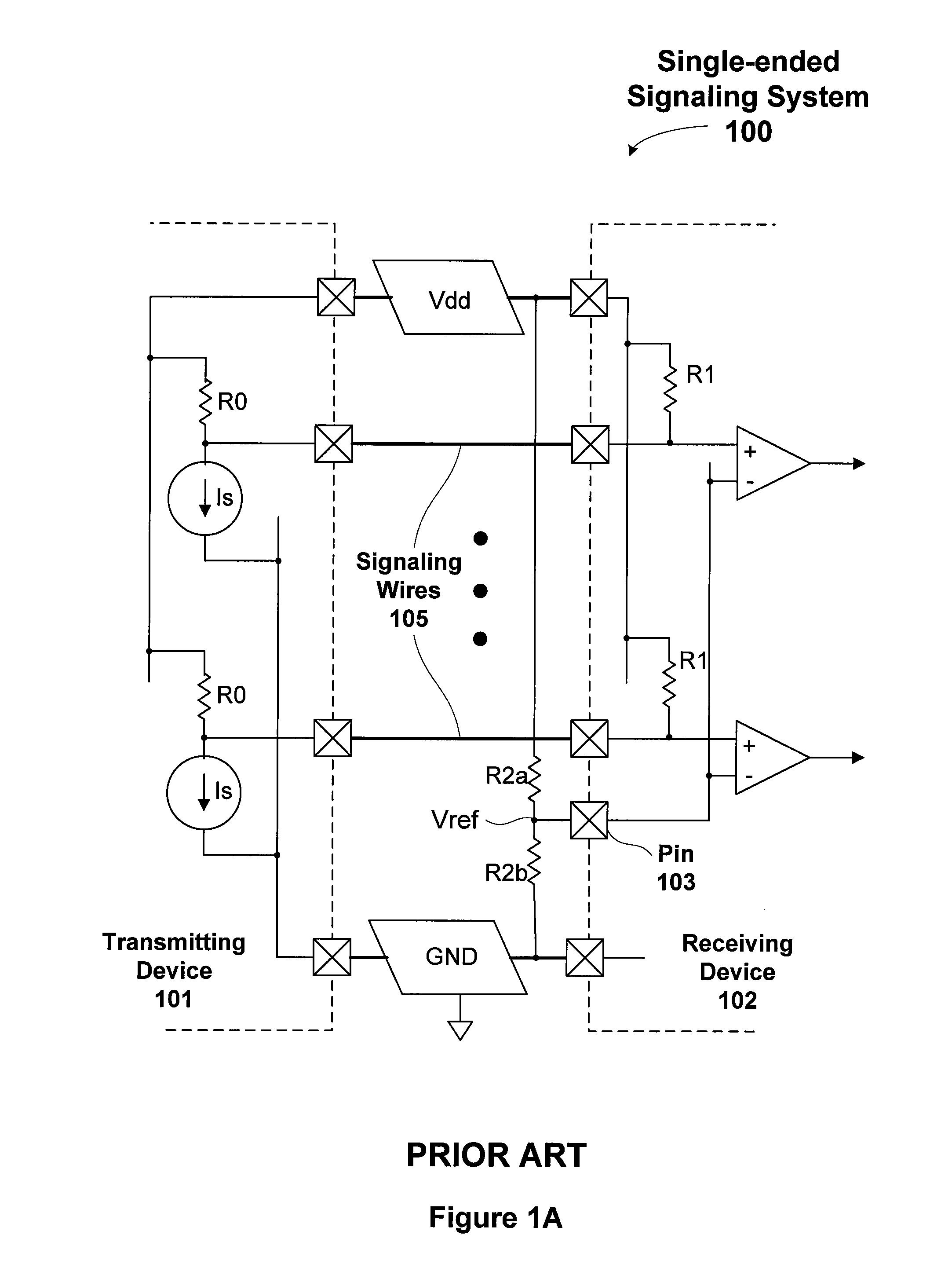
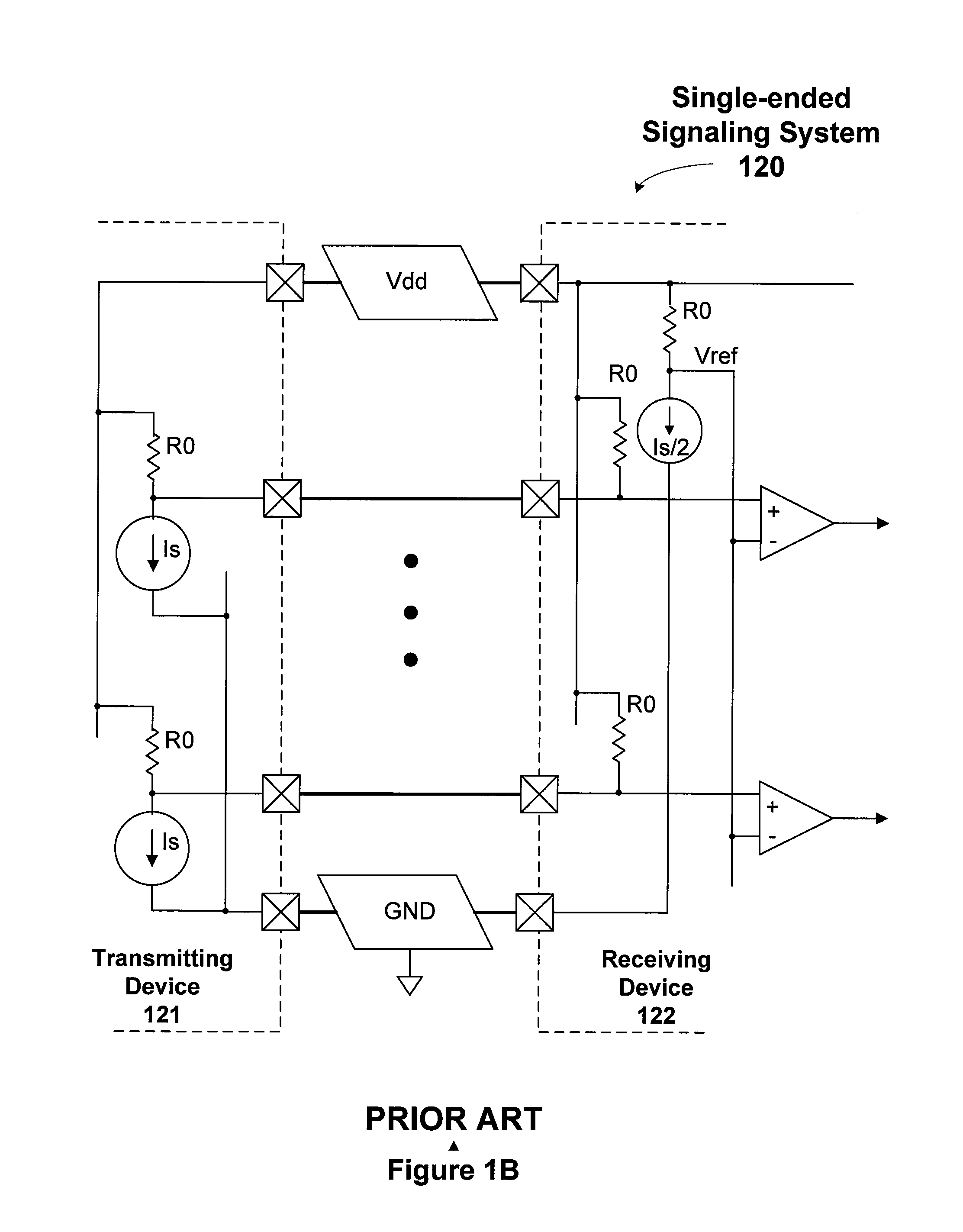
[0065]A single-ended signaling system may be constructed that uses one of the power supply networks as both the common signal return conductor and the common reference voltage. While either power supply, or even a network at a voltage level that is not used as a power supply, can be made to function as the common signal return conductor and the common reference voltage, the ground terminal is preferred, as explained further herein. Therefore, although ground-referenced signaling is described in the following paragraphs and illustrated in the Figures, the same techniques also apply to a ...
PUM
 Abstract
Description
Claims
Application Information