Photocurable Polymeric Materials and Related Electronic Devices

a technology of polymeric materials and electronic devices, applied in thermoelectric devices, photomechanical devices, instruments, etc., can solve the problems of limiting the thickness of the layer, the effect of reducing the electrical breakdown strength and high electrical breakdown strength

Active Publication Date: 2013-08-08
FLEXTERRA INC
View PDF5 Cites 25 Cited by
  • Summary
  • Abstract
  • Description
  • Claims
  • Application Information

AI Technical Summary

Benefits of technology

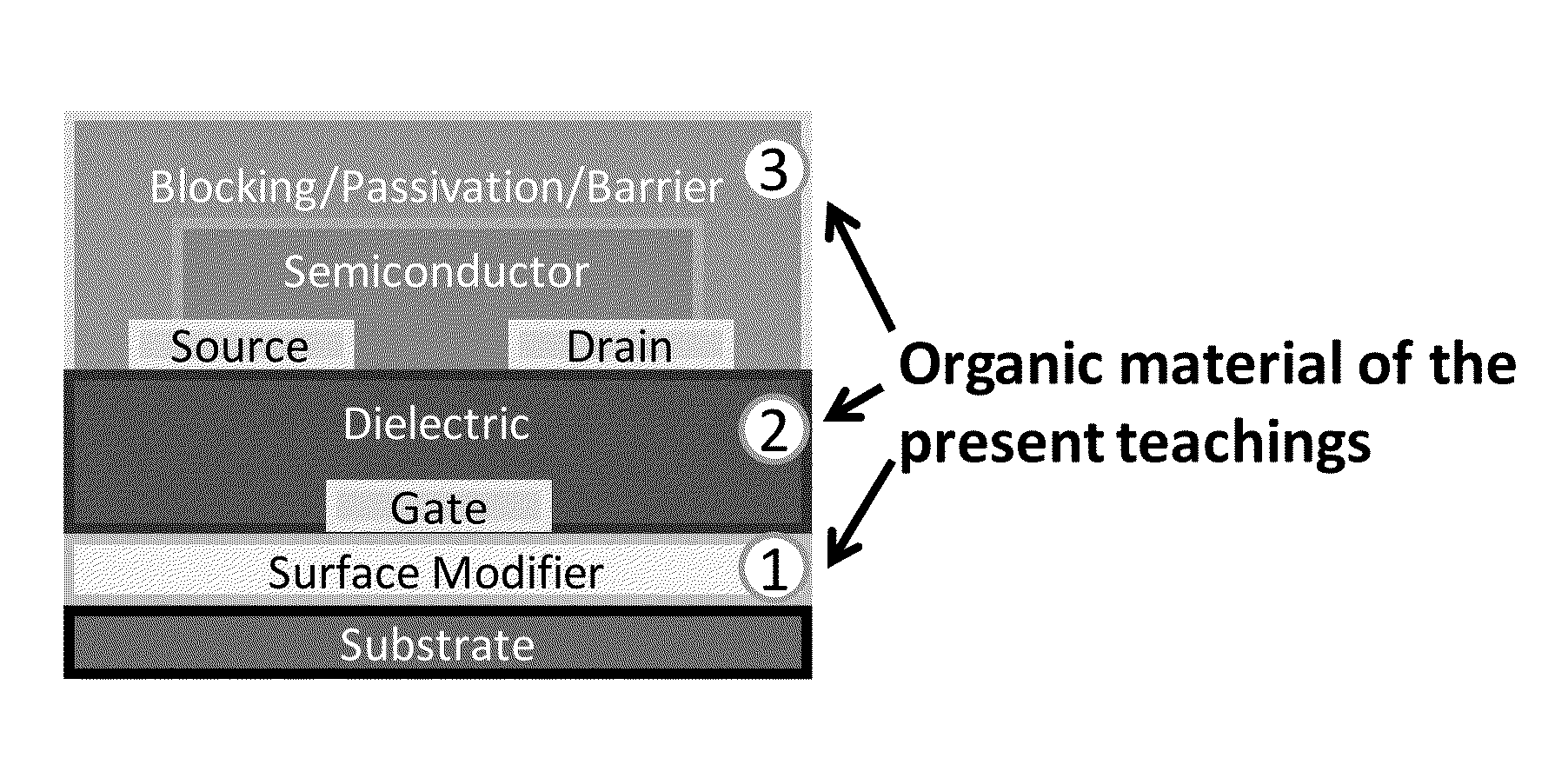
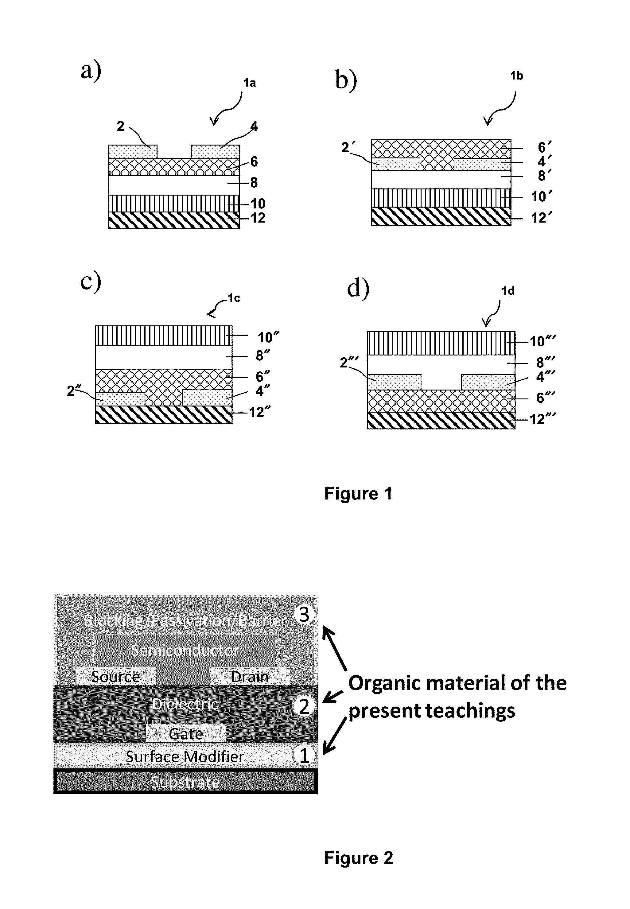
[0007]In light of the foregoing, the present teachings provide organic materials that possess one or more desirable properties and characteristics such as resistance against gate bias stress, high electrical breakdown strength, and low-leakage properties, making them suitable as gate dielectric materials in a transistor device. Certain desirable properties and characteristics of the present organic materials such as air and water stability and photocrosslinkability at low dosage and improved speed also make them suitable as barrier / passivation or photoresist materials.

Problems solved by technology

Specifically, one of the challenges for the successful commercialization of these semiconductor transistors relates to what is known as the gate bias stress effects.
Also, it is believed that water in the dielectric-semiconductor interface can cause gate bias stress effects.
However, the properties of the gate dielectric material set a limit on how thin this layer can be.

Method used


Image

  • Photocurable Polymeric Materials and Related Electronic Devices
  • Photocurable Polymeric Materials and Related Electronic Devices
  • Photocurable Polymeric Materials and Related Electronic Devices

Examples


example 1

Polymer Synthesis

Example 1a

Synthesis of P(DM-CydEMA)

[0115]

Step 1: Preparation of 2 (ethyl dimethoxy-cinnamylideneacetate)

[0116]To a suspension of NaH (60% dispersion in mineral oil, 1.39 g, 34.75 mmol) in 30 mL of anhydrous DMF was slowly added a solution of triethyl 4-phosphonocrotonate (7.7 mL, 34.75 mmol) in anhydrous DMF (20 mL). The resulting mixture was stirred at room temperature for 30 min under nitrogen and then a solution of 1 (2,5-dimethoxybenzaldehyde) (5.25 g, 31.59 mmol) in 20 mL of anhydrous DMF was added. The reaction mixture was stirred at room temperature for 15 h and then quenched with water. Ethyl acetate was added and the organic phase was separated, dried over Na2SO4, concentrated on the rotary evaporator to yield the crude compound as a yellow oil. The crude was purified by column chromatography (silica gel, hexanes:ethyl acetate (4:1, v / v)) to give compound 2 (ethyl dimethoxy-cinnamylideneacetate) as a bright yellow solid (6.23 g, 75.1% yield).

[0117]1H NMR (5...

example 1b

Synthesis of P(DM-Cyd / Acetyl(0.8:0.2)EMA)

[0124]

[0125]Poly(hydroxyethyl methacrylate) (1.0 g, Mw=20,000 g / mol, hydroxy group: 7.68 mmol) was dissolved in 5.0 mL of anhydrous pyridine. A solution of 4 (dimethoxy-cinnamylideneacetyl chloride) (1.55 g, 6.14 mmol, 0.8 equiv.) in 10.0 mL of anhydrous THF was slowly added to this polymer solution. The reaction mixture was stirred at room temperature overnight, and then a solution of acetyl chloride (0.3 g, 3.84 mmol, 0.5 equiv.) in THF was added, and the reaction was stirred for an additional 10 h. The reaction mixture was precipitated into ˜100 mL of ice-cooled methanol (MeOH). The polymer precipitates were collected and purified by two additional dissolution-precipitation steps (THF / MeOH) to yield poly(dimethoxy-cinnamylideneacetyl / acetyl(0.8:0.2)ethylmethacrylate) P(DM-Cyd / Acetyl(0.8:0.2)EMA) as a yellow solid.

example 1c

Synthesis of P(CydEMA)

[0126]

Step 1: Preparation of 6 (cinnamylideneacetyl chloride)

[0127]Compound 5 (cinnamylideneacetic acid) (5.0 g, 28.7 mmol) was dissolved in 90.0 mL of anhydrous THF, and treated with oxalyl chloride (3.0 mL, 34.3 mmol) and 3 drops of DMF. The reaction mixture was stirred at room temperature for 4 h and then concentrated on a rotary evaporator to remove all the volatiles. Compound 6 (cinnamylideneacetyl chloride) was obtained as a pale yellow solid (5.0 g, 90.4% yield).

[0128]1H NMR (500 MHz, CDCl3): δ 7.65 (dd, 1H, J=7.5 Hz, 11.5 Hz), 7.54 (d, 1H, J=2.0 Hz), 7.53 (d, 1H, J=2.0 Hz), 7.44 (m, 3H), 7.11 (d, 1H, J=15.0 Hz), 6.95 (dd, 1H, J=7.5 Hz, 11.5 Hz), 6.21 (d, 1H, J=12.5 Hz).

Step 2: Preparation of poly(cinnamylideneacetylethylmethacrylate) [P(CydEMA)]

[0129]Poly(hydroxyethyl methacrylate) (1.56 g, Mw=20,000 g / mol, hydroxy group: 11.99 mmol) was dissolved in 5.0 mL of anhydrous pyridine. A solution of 6 (cinnamylideneacetyl chloride) (3.0 g, 15.57 mmol) in 10.0...


PUM

PropertyMeasurementUnit
solubilityaaaaaaaaaa

Abstract

Disclosed are photocurable polymers that can be used as active and/or passive organic materials in various electronic, optical, and optoelectronic devices. In some embodiments, the device can include a dielectric layer prepared from such photocurable polymers. In some embodiments, the device can include a passivation layer prepared from the polymers described herein.

Description

CROSS REFERENCE TO RELATED APPLICATIONS[0001]This application is a continuation of International Application No. PCT / US2013 / 025000, filed on Feb. 6, 2013, which claims priority to and the benefit of U.S. Provisional Patent Application Ser. No. 61 / 596,217, filed on Feb. 7, 2012, the disclosure of each of which is incorporated by reference herein in its entirety.INTRODUCTION[0002]In the past decade, there has been a growing interest in developing electronic devices using organic or (amorphous) metal oxide materials as the semiconductor component. These devices can offer advantages such as structural flexibility, potentially much lower manufacturing costs, and the possibility of low-temperature ambient manufacturing processes on large areas. For example, both organic and (amorphous) metal oxide materials can be used to enable new devices such as electronic paper, flexible liquid crystal display panels, flexible organic light-emitting diodes (OLEDs), and radio-frequency identification (...

Claims


Application Information

Patent Timeline
Patent Type & Authority Applications(United States)
IPC IPC(8): H01L51/05
CPCH01L51/0512G03F7/0388G03F7/092H01L51/052C08F220/30H01L51/0545H01L51/107C08F220/28H01L51/0541C08F220/20C08F220/302H10K10/471H10K10/464H10K10/88H10K10/466H10K10/462
Inventor USTA, HAKAHTAN, HUEI SHUAN PHOEBEXIA, YUCHEN, ZHIHUAZHENG, YANFACCHETTI, ANTONIO
Owner FLEXTERRA INC
Why Eureka
Try Eureka