Electrical interconnect IC device socket

a technology of electric interconnection and device socket, which is applied in the direction of printed circuit manufacturing, printed circuit aspects, printed element electric connection formation, etc., can solve the problems of increasing contact resistance, reducing signal integrity, and long contact members reducing signal integrity

Active Publication Date: 2013-08-15
HSIO TECH
View PDF2 Cites 59 Cited by
  • Summary
  • Abstract
  • Description
  • Claims
  • Application Information

AI Technical Summary

Benefits of technology

[0007]The present disclosure is directed to a surface mount BGA device socket that will enable next generation electrical performance. The present solution removes the normal retention features, which add parasitic mass and distort or degrade the integrity of the signal as it passes through the contact. This approach provides a reliable connection to BGA devices and creates a platform to add electrical and mechanical enhancements to the socket substrate or assembly to address the challenges of next generation interconnect requirements.

Problems solved by technology

As IC devices advance to next generation architectures traditional IC sockets have reached mechanical and electrical limitations that require alternate methods.
Longer contact members also tend to reduce signal integrity and increase contact resistance due to self-heating of power delivering contacts.
The thinner insulating walls increase the difficulty of molding and increase latent stresses in the IC socket housing, increasing the risk of warpage during solder reflow.
The thinner insulating walls also increase the risk of cross-talk between adjacent contact members.
Traditional IC sockets have reached an electrical performance limit.
Next generation IC devices will operate above 5 GHz and beyond and the existing IC sockets do not provide acceptable performance levels without significant revision.

Method used


Image

  • Electrical interconnect IC device socket
  • Electrical interconnect IC device socket
  • Electrical interconnect IC device socket

Examples


Embodiment Construction

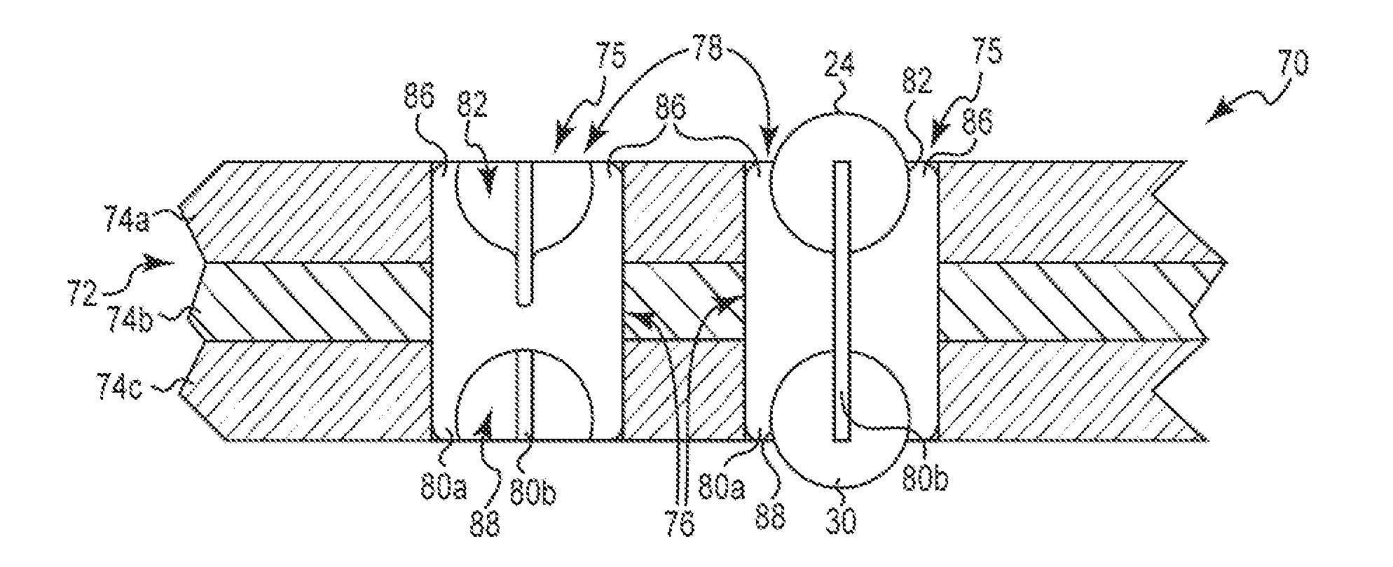
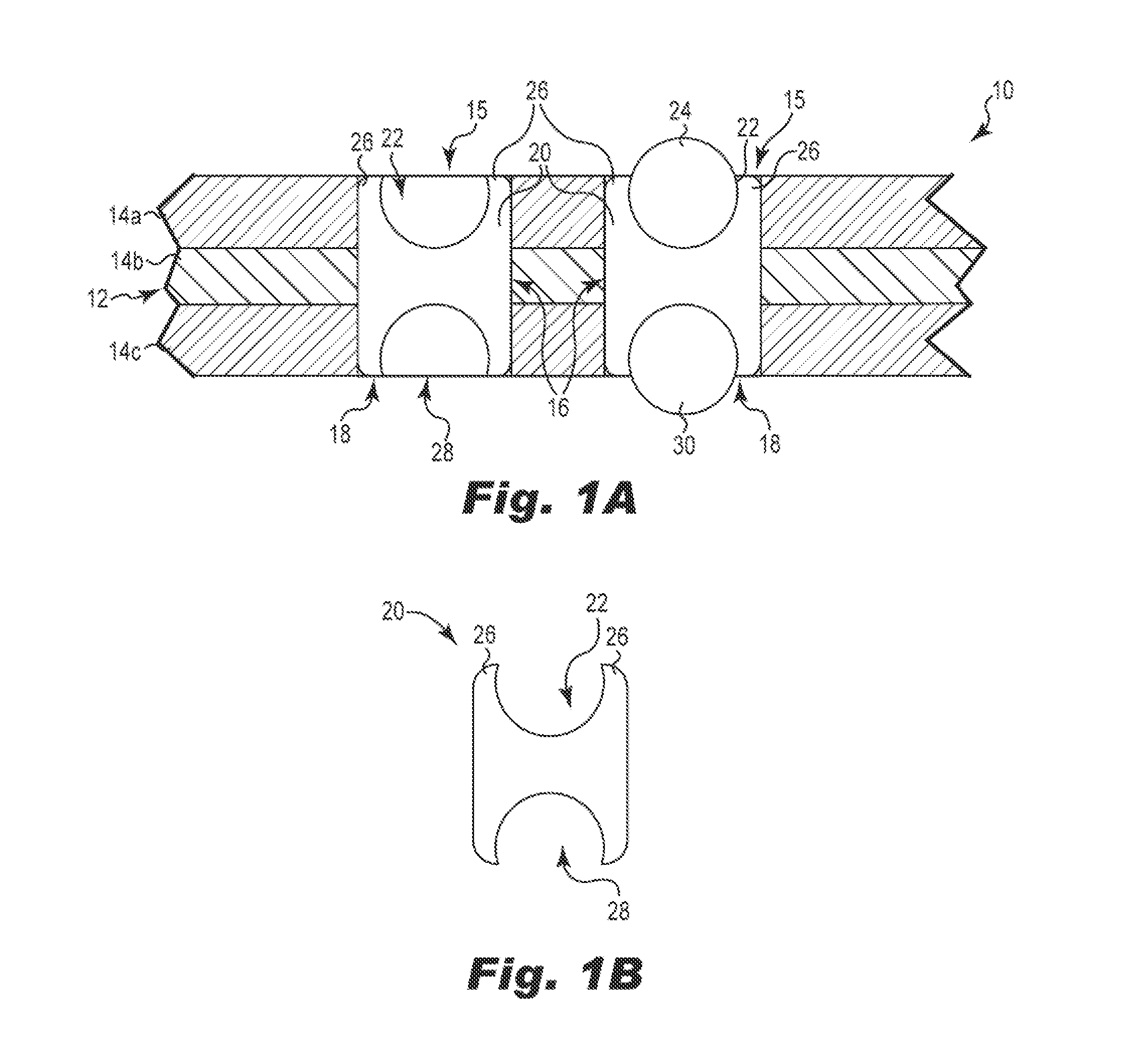
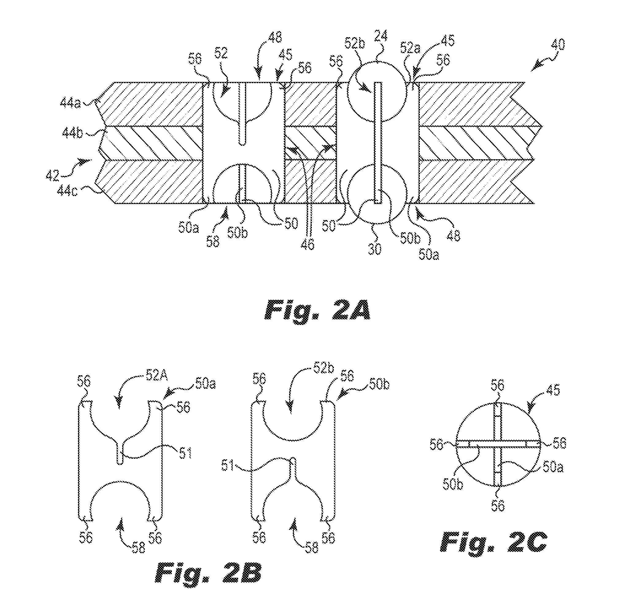
[0053]A high performance electrical interconnect according to the present disclosure may permit fine contact-to-contact spacing (pitch) on the order of less than 1.0 mm pitch, and more preferably a pitch of less than about 0.7 millimeter, and most preferably a pitch of less than about 0.4 millimeter. Such fine pitch high performance electrical interconnects are especially useful for communications, wireless, and memory devices.

[0054]The present high performance electrical interconnect can be configured as a low cost, high signal performance interconnect assembly, which has a low profile that is particularly useful for desktop and mobile PC applications. IC devices can be installed and uninstalled without the need to reflow solder. The solder-free electrical connection of the IC devices is environmentally friendly.

[0055]The embodiments of the present disclosure may enable a user to directly socket a ball grid array (“BGA”) device to a printed circuit board (“PCB”) without reflowing s...


PUM

PropertyMeasurementUnit
aspect ratioaaaaaaaaaa

Abstract

A surface mount electrical interconnect is disclosed that provides an interface between a PCB and solder balls of a BGA device. The electrical interconnect includes a socket substrate and a plurality of electrically conductive contact members. The socket substrate has a first layer with a plurality of openings configured to receive solder balls of the BGA device and has a second layer with a plurality of slots defined therethrough that correspond to the plurality of openings. The contact members may be disposed in the openings in the first layer and through the plurality of slots of the second layer of the socket substrate. The contact members can be configured to engage a top portion, a center diameter, and a lower portion of the solder ball of the BGA device. Each contact member electrically couples a solder ball on the BGA device to the PCB.

Description

TECHNICAL FIELD[0001]The present disclosure relates to an electrical interconnect integrated circuit (“IC”) device socket, and, in particular, to a surface mount ball grid array (“BGA”) device socket. The present disclosure also discloses the use of unique fabrication techniques that merge processes used in the printed circuit and semiconductor packaging industries with the flexibility of additive printing technology to make the present surface mount electrical interconnect.BACKGROUND OF THE INVENTION[0002]Traditional IC sockets are generally constructed of an injection molded plastic insulator housing that includes stamped and formed copper alloy contact members stitched or inserted into recesses. The assembled IC socket is then generally processed through a reflow oven to attach solder balls to the contact members. During final assembly the contact pads on the printed circuit board (“PCB”) are printed with solder paste or flux and the solder balls on the IC socket are placed in re...

Claims


Application Information

Patent Timeline
Patent Type & Authority Applications(United States)
IPC IPC(8): H05K1/02H05K3/40
CPCH01R43/0256H05K1/141H05K3/3436H05K3/3484H05K3/4046Y10T29/49147H05K2203/041H05K1/0228H05K1/0296H05K3/40H05K2201/10378H05K3/3485
Inventor RATHBURN, JAMES
Owner HSIO TECH
Why Eureka
Try Eureka