Semiconductor device

a semiconductor and memory device technology, applied in the direction of solid-state devices, instruments, digital data processing details, etc., can solve the problems of low-reliability data of the memory device, stop power supply, increase the power consumption of the cpu, etc., to achieve high data reliability, low power consumption in data write, and high speed

Active Publication Date: 2013-08-29
SEMICON ENERGY LAB CO LTD
View PDF12 Cites 40 Cited by
  • Summary
  • Abstract
  • Description
  • Claims
  • Application Information

AI Technical Summary

Benefits of technology

[0027]According to one embodiment of the present invention, a memory device from which highly reliable data is obtained can be provided. According to one embodiment of the present invention, a memory device whose power consumption in data write can be low and which is nonvolatile and writes data at a high speed can be provided. According to one embodiment of the present invention, a highly reliable semiconductor device can be provided. According to one embodiment of the present invention, a semiconductor device whose power consumption is low can be provided.

Problems solved by technology

The above memory device has a problem in that a short period of stopping the supply of power is likely to result in an increase in power consumption of a CPU when a period of stopping the supply of power in which an electric power consumed by saving and restoring of data (overhead) and an electric power saved by stopping the supply of power are equal to each other, that is, a break even time (BET) is long.
However, the volatile memory element generally includes a flip-flop, and the potential of any node between semiconductor elements included in a flip-flop is in an indefinite state while the supply of power is stopped.
Consequently, the stop of the supply of power is likely to generate low-reliability data of the memory device.

Method used


Image

  • Semiconductor device
  • Semiconductor device
  • Semiconductor device

Examples


embodiment 1

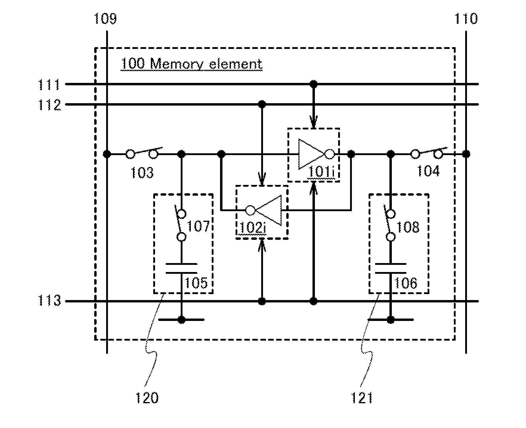
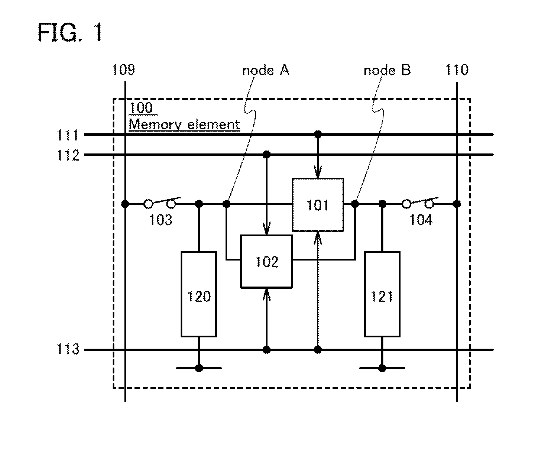
[0047]A memory device according to one embodiment of the present invention includes at least one memory element 100 capable of storing one-bit data. FIG. 1 shows the structure of the memory element 100.

[0048]The memory element 100 includes a logic element 101, a logic element 102, a switch 103, a switch 104, a memory circuit 120, and a memory circuit 121.

[0049]The logic elements 101 and 102 each have a function of inverting the polarity of the potential of an input terminal to output the potential from an output terminal. That is, the logic elements 101 and 102 each have a function of inverting a logic level of a signal. Specifically, the logic elements 101 and 102 each can be an inverter, a clocked inverter, or the like. In addition, the input terminal of the logic element 101 is connected to the output terminal of the logic element 102, and the input terminal of the logic element 102 is connected to the output terminal of the logic element 101.

[0050]The memory element 100 is conne...

embodiment 2

[0132]In this embodiment, a specific embodiment of a CPU corresponding to one mode of a semiconductor device of the present invention will be described. FIG. 8 is a block diagram illustrating a structure example of a CPU. Although the block diagram attached this specification shows elements classified according to their functions in independent blocks, it may be practically difficult to completely separate the elements according to their functions and, in some cases, one element may be involved in a plurality of functions.

[0133]A CPU 600 includes a controller 601, an arithmetic logic unit (ALU) 602 corresponding to an arithmetic unit, a data cache 603, an instruction cache 604, a program counter 605, an instruction register 606, a main storage device 607, and a register file 608.

[0134]The control unit 601 has functions of decoding and executing an input instruction. The ALU 602 has a function of performing a variety of arithmetic operations such as four arithmetic operations and log...

embodiment 3

[0163]In this embodiment, an example of a cross sectional structure of a memory device that includes the memory element 100 illustrated in FIG. 5 will be described. Note that in this embodiment, the case where the transistors 103t, 104t, and 114 to 117 each include an active layer containing an amorphous, microcrystalline, polycrystalline, or single crystal semiconductor (e.g., silicon or germanium) and the transistors 107t and 108t each include an active layer containing an oxide semiconductor is given as an example to describe a cross sectional structure of the memory element 100.

[0164]As a silicon, any of the following can be used: amorphous silicon manufactured by a vapor phase growth method such as a plasma CVD method, or a sputtering method; polycrystalline silicon obtained in such a manner that amorphous silicon is crystallized by treatment such as laser annealing; single crystal silicon obtained in such a manner that implantation of hydrogen ions or the like into a silicon w...


PUM


Abstract

The memory device includes a first logic element which is supplied with a first power supply voltage, and inverts a polarity of a potential of an input terminal to output the potential with the inverted polarity from an output terminal, a second logic element which is supplied with a second power supply voltage supplied through a different path from the first power supply voltage, and inverts a polarity of a potential of an input terminal to output the potential with the inverted polarity from an output terminal, a first memory circuit connected to the input terminal of the first logic element, and a second memory circuit connected to the input terminal of the second logic element. The input terminal and the output terminal of the first logic element are connected to the output terminal and the input terminal of the second logic element, respectively.

Description

BACKGROUND OF THE INVENTION[0001]1. Field of the Invention[0002]The present invention relates to a memory device and a semiconductor device including the memory device.[0003]2. Description of the Related Art[0004]Semiconductor elements of semiconductor devices such as central processing units (CPUs) has been downsized to increase operation speed and integration degree, and now transistors with a channel length of approximately 30 nm are manufactured. On the other hand, downsizing semiconductor elements leads to an increase in power consumption (leakage power) due to leakage current of transistors in CPUs. Specifically, most of power consumption of conventional CPUs is power consumption (operation power) at the time of calculations, while leakage power accounts for at least 10% of power consumption of CPUs in recent years.[0005]In particular, a cache often has large capacity to achieve high CPU throughput, and corresponds to an integrated circuit whose leakage power is the largest am...

Claims


Application Information

Patent Timeline
Patent Type & Authority Applications(United States)
IPC IPC(8): G11C5/14G11C11/24
CPCG11C11/412G11C11/419G11C11/24G11C5/14G06F1/3275Y02D10/00H01L27/1214H01L27/1225H01L27/1255
Inventor KOYAMA, JUN
Owner SEMICON ENERGY LAB CO LTD
Why Eureka
Try Eureka