Copper foil for printed wiring board

a technology of copper foil and printed wiring, which is applied in the direction of superimposed coating process, vacuum evaporation coating, transportation and packaging, etc., can solve the problems of conflicting etching performance and corrosion resistance, and reducing adhesion (corrosion resistance), so as to improve the adhesion to the insulating substrate and etching performance. , the effect of excellent etching performance and superior manufacturing cos

Active Publication Date: 2013-09-19
JX NIPPON MINING& METALS CORP
View PDF10 Cites 2 Cited by
  • Summary
  • Abstract
  • Description
  • Claims
  • Application Information

AI Technical Summary

Benefits of technology

[0037]It is possible to obtain a copper foil for a printed wiring board that is excellent in both of adhesiveness to

Problems solved by technology

However, since the magnetic target has poor efficiency and a short life, there is a problem in that this technique is disadvantageous in terms of cost.
In addition, in Patent document 1 (JP 2006-222185 A), a reduction in adhesion (corrosion resistance) due to the reaction of the surface-treat

Method used


Image

  • Copper foil for printed wiring board
  • Copper foil for printed wiring board
  • Copper foil for printed wiring board

Examples


examples

[0079]Hereinafter, examples of the invention will be shown, but these are provided only to understand the invention better rather than to limit the invention.

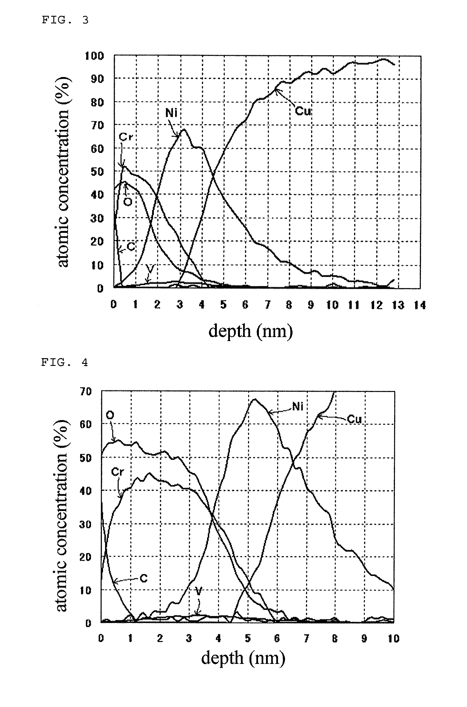
[0080]A rolled copper foil (C1100 manufactured by JX Nippon Mining & Metals Corporation) having a thickness of 17 μm and an electrolytic copper foil not subjected to a roughening treatment were provided as copper foil base materials. The surface roughnesses (Rz) of the rolled copper foil and the electrolytic copper foil were 0.7 μm and 1.5 μm, respectively.

[0081]A Ni—V alloy layer and a Cr layer were formed in order on one side of the copper foil after a thin oxide film attached to a surface of the copper foil base material was removed in advance by reverse sputtering under the following conditions. The thickness of the coating layer was changed by adjusting a film forming time.

[0082]Device: Batch-Type Sputter (Ulvac, Inc., Type: MNS-6000)

[0083]Ultimate Vacuum: 1.0×10⁻⁵ Pa

[0084]Sputtering Pressure: 0.2 Pa

[0085]Reverse Sputterin...


PUM

PropertyMeasurementUnit
Temperatureaaaaaaaaaa

Abstract

Provided is a copper foil for a printed wiring board, the copper foil being suitable for achieving finer pitch, favorable in terms of manufacturing cost, and excellent both in etching ability and adhesion to an insulating substrate. The copper foil for a printed wiring board comprises a copper foil base material and a covering layer for covering at least a portion of a surface of the copper foil base material, wherein the covering layer is formed by an nickel-vanadium alloy layer containing nickel and vanadium, and a chromium layer, laminated in this order from the surface of the copper foil base material; the chromium layer contains chromium in an amount of 15-210 μg/dm2; the nickel-vanadium alloy layer contains nickel and vanadium in a combined covering amount of 20-600 μg/dm2; and the nickel-vanadium alloy layer contains vanadium in an amount of 3-70 wt %.

Description

BACKGROUND[0001]1. Technical Field[0002]The present invention relates to a copper foil for a printed wiring board, and particularly, to a copper foil for a flexible printed wiring board.[0003]2. Related Art[0004]Printed wiring boards have been significantly developed for the last half century, and these days, the printed wiring boards escalate in almost all of electronics. High-density packaging of components to be mounted thereon and raising a signal frequency have been progressed together with increasing needs to downsize and offer high performance to electronics in recent years, and printed wiring boards are required to have miniaturization in conductive patterns (fine pitch), high frequency solutions, and the like.[0005]Generally, printed wiring boards are manufactured through the steps of: adhering an insulating substrate to a copper foil to form a copper-clad laminate; and forming a conductive pattern on the copper foil surface by etching. Therefore, copper foils for a printed...

Claims


Application Information

Patent Timeline
IPC IPC(8): H05K1/09
CPCC23C14/165C23C28/023H05K1/0393H05K3/022H05K3/384Y10T428/12569H05K1/09Y10T428/12438Y10T428/1291Y10T428/12819C23C26/00
Inventor TANAKA, KOICHIROCHUGANJI, MISATO
Owner JX NIPPON MINING& METALS CORP
Why Eureka
Try Eureka