Method of enabling seamless cobalt gap-fill

a cobalt gap and cobalt technology, applied in the direction of semiconductor devices, semiconductor/solid-state device details, electrical equipment, etc., can solve the problems of device shorting or poor interconnection formation, poor step coverage of contact metal layer deposited using a conventional pvd process, and void formation within the via or trench,

Active Publication Date: 2013-10-03
APPLIED MATERIALS INC
View PDF26 Cites 109 Cited by
  • Summary
  • Abstract
  • Description
  • Claims
  • Application Information

AI Technical Summary

Problems solved by technology

However, as the limits of integrated circuit technology are pushed, the shrinking dimensions of interconnects in VLSI and ULSI technology have placed additional demands on processing capabilities.
A variety of problems may occur when depositing contact metal layers into contact structures with small geometries, such as geometries having aspect ratios of about 20:1 or smaller.
For example, a contact metal layer deposited using a conventional PVD process often suffers from poor step coverage, overhang, and voids formed within the via or trench when the via has a critical dimension of less than 50 nm or has an aspect ratio greater than 10:1.
Insufficient deposition on the bottom and sidewalls of the vias or trenches can also result in deposition discontinuity, thereby resulting in device shorting or poor interconnection formation.
Furthermore, the contact metal layer may have poor adhesion over the underlying silicon containing layer, resulting in peeling of the contact metal layer from the substrate and the subsequent conductive metal layer.
With this increase in transistor density and subsequent decrease in the cross-sections of metal-contacts, meeting the contact resistance requirements using existing low resistivity tungsten (W) integration schemes has become quite challenging.
The necessity of high-resistivity adhesion (e.g., B2H6 nucleation) and barrier layers (e.g., TiN) in the tungsten contact integration scheme results in increased contact resistance making it an unattractive option for technology nodes less than 22 nanometers.

Method used


Image

  • Method of enabling seamless cobalt gap-fill
  • Method of enabling seamless cobalt gap-fill
  • Method of enabling seamless cobalt gap-fill

Examples


Embodiment Construction

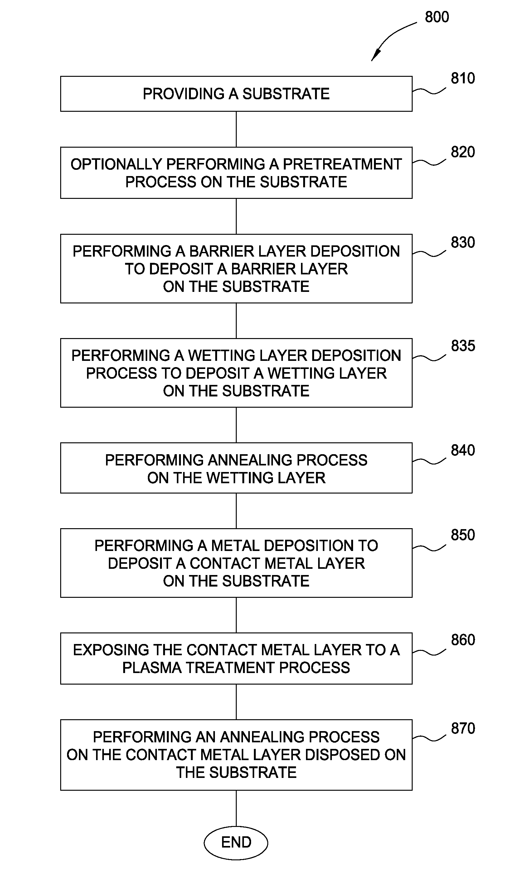
[0022]Embodiments of the present invention provide gap-fill utilizing metallic CVD processes (e.g., cobalt CVD processes) resulting in a potential low contact resistance (Rc) one-material solution for contact fill. The CVD films deposited according to embodiments described herein have conformal step coverage and low surface roughness. Further, the embodiments demonstrated herein demonstrate a process for filling contact holes of a semiconductor device with no seam formation.

[0023]In one embodiment, a method for depositing a contact metal layer over a substrate is provided which includes exposing the substrate to a cobalt precursor gas and hydrogen gas to selectively form a portion of a seamless gap fill cobalt layer within a feature, and exposing the cobalt layer to a plasma and a reagent, such as nitrogen, ammonia, hydrogen, an ammonia / nitrogen mixture, or combinations thereof during a post-treatment process.

[0024]As will be explained in greater detail below, a contact metal layer ...


PUM

PropertyMeasurementUnit
diameteraaaaaaaaaa
diameteraaaaaaaaaa
diameteraaaaaaaaaa

Abstract

Methods for depositing a contact metal layer in contact structures of a semiconductor device are provided. In one embodiment, a method for depositing a contact metal layer for forming a contact structure in a semiconductor device is provided. The method comprises performing a cyclic metal deposition process to deposit a contact metal layer on a substrate and annealing the contact metal layer disposed on the substrate. The cyclic metal deposition process comprises exposing the substrate to a deposition precursor gas mixture to deposit a portion of the contact metal layer on the substrate, exposing the portion of the contact metal layer to a plasma treatment process, and repeating the exposing the substrate to a deposition precursor gas mixture and exposing the portion of the contact metal layer to a plasma treatment process until a predetermined thickness of the contact metal layer is achieved.

Description

CROSS-REFERENCE TO RELATED APPLICATIONS[0001]This application claims benefit of U.S. provisional patent application No. 61 / 616,842, filed Mar. 28, 2012, which is hereby incorporated by reference.BACKGROUND OF THE INVENTION[0002]1. Field of the Invention[0003]Embodiments of the invention generally relate to the field of semiconductor manufacturing processes, more particularly, to methods for depositing a contact metal layer in contact structures of a semiconductor device.[0004]2. Description of the Related Art[0005]Integrated circuits may include more than one million micro-electronic field effect transistors (e.g., complementary metal-oxide-semiconductor (CMOS) field effect transistors) that are formed on a substrate (e.g., semiconductor wafer) and cooperate to perform various functions within the circuit. Reliably producing sub-half micron and smaller features is one of the key technologies for the next generation of very large scale integration (VLSI) and ultra large-scale integra...

Claims


Application Information

Patent Timeline
Patent Type & Authority Applications(United States)
IPC IPC(8): H01L21/48
CPCH01L21/4846H01L21/76883H01L21/2855H01L21/28556H01L21/02057H01L21/76843H01L21/76846H01L21/76856H01L21/76814H01L21/76877H01L29/66621H01L23/53209H01L21/76879H01L23/5329
Inventor ZOPE, BHUSHAN N.GELATOS, AVGERINOS V.ZHENG, BOLEI, YUFU, XINYUGANDIKOTA, SRINIVASYU, SANG-HOABRAHAM, MATHEW
Owner APPLIED MATERIALS INC
Why Eureka
Try Eureka