Method of enabling seamless cobalt gap-fill

a cobalt gap and cobalt technology, applied in the direction of semiconductor/solid-state device details, chemical vapor deposition coating, coating, etc., can solve the problems of device shorting or poor interconnection formation, poor adhesion, and poor step coverage of metal layer deposited using a conventional pvd process

Active Publication Date: 2015-04-02
APPLIED MATERIALS INC
View PDF9 Cites 176 Cited by
  • Summary
  • Abstract
  • Description
  • Claims
  • Application Information

AI Technical Summary

Problems solved by technology

However, as the limits of integrated circuit technology are pushed, the shrinking dimensions of interconnects in VLSI and ULSI technology have placed additional demands on processing capabilities.
A variety of problems may occur when depositing metal layers into feature definitions with small geometries, such as geometries having aspect ratios of about 20:1 or smaller.
For example, a metal layer deposited using a conventional PVD process often suffers from poor step coverage, overhang, and voids formed within the via or trench when the via has a critical dimension of less than 50 nm or has an aspect ratio greater than 10:1.
Insufficient deposition on the bottom and sidewalls of the vias or trenches can also result in deposition discontinuity, thereby resulting in device shorting or poor interconnection formation.
Furthermore, the metal layer may have poor adhesion over the underlying material layer, resulting in peeling of the metal layer from the substrate and the subsequent conductive metal layer.
With this increase in transistor density and subsequent decrease in the cross-sections of metal layers, meeting the contact resistance requirements using existing low resistivity tungsten (W) integration schemes has become quite challenging.
The necessity of high-resistivity adhesion (e.g., B2H6 nucleation) and barrier layers (e.g., TiN) in the tungsten integration scheme results in increased contact resistance making it an unattractive option for technology nodes less than 22 nanometers.

Method used


Image

  • Method of enabling seamless cobalt gap-fill
  • Method of enabling seamless cobalt gap-fill
  • Method of enabling seamless cobalt gap-fill

Examples


Embodiment Construction

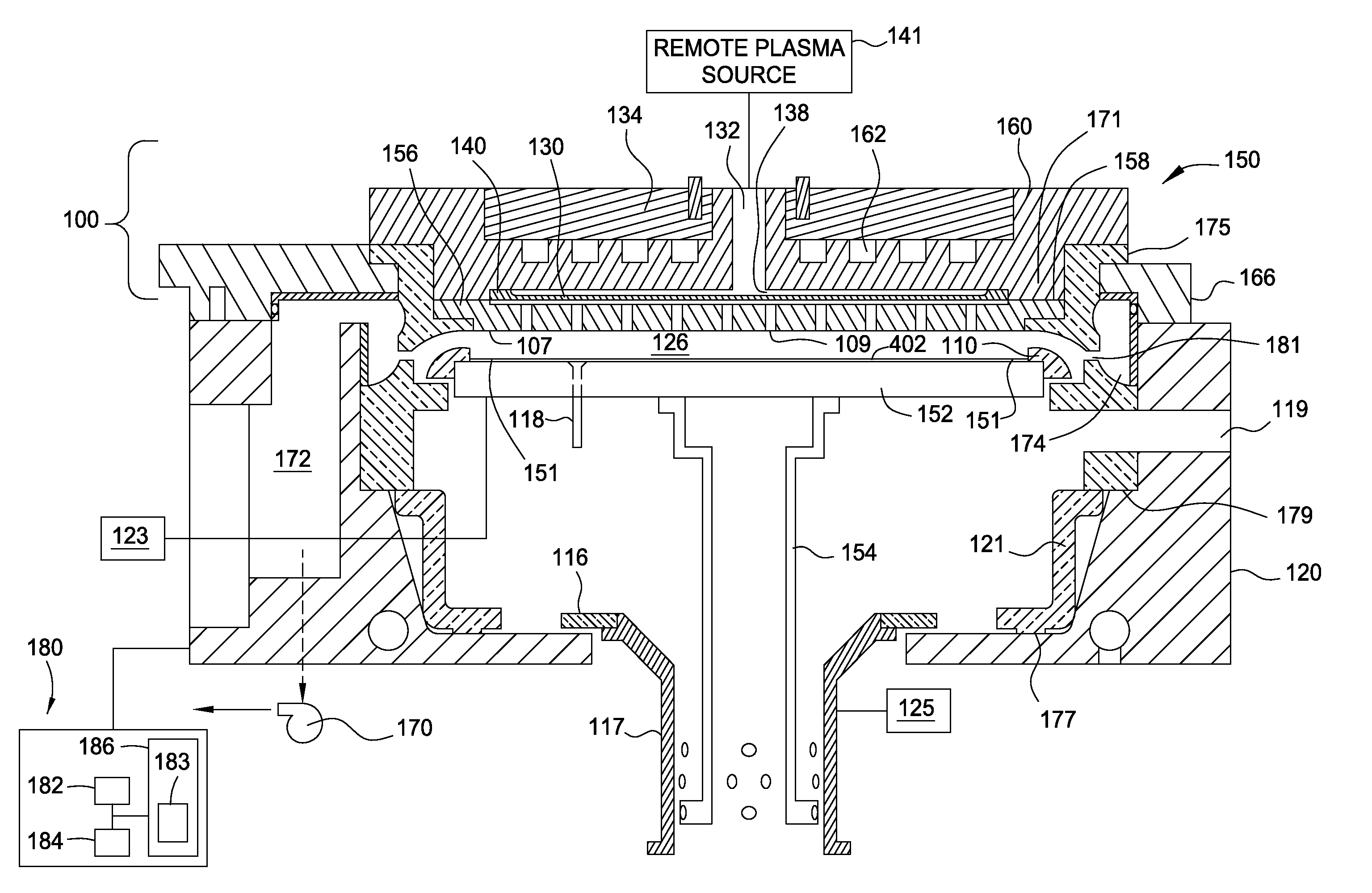
[0024]The increase in transistor density combined with the shrinking technology nodes (≦11 nm) of advanced CMOS transistors has resulted in decrease in the cross-section dimensions of conducting metal layers utilized during semiconductor manufacturing. Examples of such metal conducting layers include metal contact fill, metal gate fill and interconnect fill, Very narrow cross-section dimensions (2 nm) high resistivity barrier layers. Gap-fill methods utilizing CVD cobalt processes provides a potential low contact resistance (Rc) one-material solution for gap-fill. The CVD cobalt films are required to have conformal step coverage and low roughness. Certain implementations described herein demonstrate a process to fill conducting layer holes or trenches of a semiconductor device with no seam formation.

[0025]In some implementations, the purity of the cobalt film was found to govern cobalt seamless fill. The atomic % of carbon, nitrogen & oxygen impurities in the CVD cobalt film may be ...


PUM

PropertyMeasurementUnit
pressureaaaaaaaaaa
temperatureaaaaaaaaaa

Abstract

Methods for depositing a metal layer in a feature definition of a semiconductor device are provided. In one implementation, a method for depositing a metal layer for forming a semiconductor device is provided. The method comprises performing a cyclic metal deposition process to deposit a metal layer on a substrate and annealing the metal layer disposed on the substrate. The cyclic metal deposition process comprises exposing the substrate to a deposition precursor gas mixture to deposit a portion of the metal layer on the substrate, exposing the portion of the metal layer to either a plasma treatment process or hydrogen annealing process and repeating the exposing the substrate to a deposition precursor gas mixture and exposing the portion of the metal layer to either a plasma treatment process or hydrogen annealing process until a predetermined thickness of the metal layer is achieved.

Description

CROSS-REFERENCE TO RELATED APPLICATIONS[0001]This application claims benefit of U.S. provisional patent application Ser. No. 61 / 883,480, filed Sep. 27, 2013. The aforementioned related patent application is herein incorporated by reference in its entirety.BACKGROUND[0002]1. Field[0003]Implementations of the disclosure generally relate to the field of semiconductor manufacturing processes, more particularly, to methods for depositing metal containing layers in features of a semiconductor device.[0004]2. Description of the Related Art[0005]Integrated circuits may include more than one million micro-electronic field effect transistors (e.g., complementary metal-oxide-semiconductor (CMOS) field effect transistors) that are formed on a substrate (e.g., semiconductor wafer) and cooperate to perform various functions within the circuit. Reliably producing sub-half micron and smaller features is one of the key technologies for the next generation of very large scale integration (VLSI) and u...

Claims


Application Information

Patent Timeline
Patent Type & Authority Applications(United States)
IPC IPC(8): H01L21/768
CPCH01L21/768H01L21/76877H01L21/7684H01L21/28562H01L21/76814H01L21/76843H01L21/76876C23C16/18H01L23/53209H01L21/2855H01L21/28568H01L21/76879H01L21/76883
Inventor ZOPE, BHUSHAN N.GELATOS, AVGERINOS V.ZHENG, BOLEI, YUFU, XINYUGANDIKOTA, SRINIVASYU, SANG HOABRAHAM, MATHEW
Owner APPLIED MATERIALS INC
Why Eureka
Try Eureka