Thin film transistor memory and its fabricating method

a technology of thin film transistors and manufacturing methods, applied in the direction of basic electric elements, electrical equipment, semiconductor devices, etc., can solve the problems of large variation on threshold voltage, poor program/erase efficiency and data retention of tft memories based on polycrystalline silicon, and many restrictions, so as to improve data retention, increase storage charge density, and extend the program/erase window

Inactive Publication Date: 2013-10-10
FUDAN UNIV
View PDF4 Cites 9 Cited by
  • Summary
  • Abstract
  • Description
  • Claims
  • Application Information

AI Technical Summary

Benefits of technology

[0034]1) Using two-layer metal nanocrystals as the charge storage layer can increase the storage charge density, extend the program/erase window and improve the data retention.
[0035]2) Using the symmetrical stack layer as tunneling layer can improve the program/erase speed and decrease the working voltage without infecting the data retention.
[0036]3) Using the amorphous IGZO film can provide the uniform carriers mobility and stable electrical performance. In addition, this invention has a good. prospect in the transparent and flexible electrical devices due to the high transparency and low process temperature of IGZO film.
[0037]4) Using ALD method can grow the metal nanocrystals below 400° C., thus it decreases the...

Problems solved by technology

However, the traditional nonvolatile floating gate memories fabricated on monocrystalline silicon substrate are difficult to fabricate on the glass substrate due to the complicated fabricating method and high process temperature, and that will lead them subject to many restrictions when they a...

Method used


Image

  • Thin film transistor memory and its fabricating method
  • Thin film transistor memory and its fabricating method
  • Thin film transistor memory and its fabricating method

Examples


Embodiment Construction

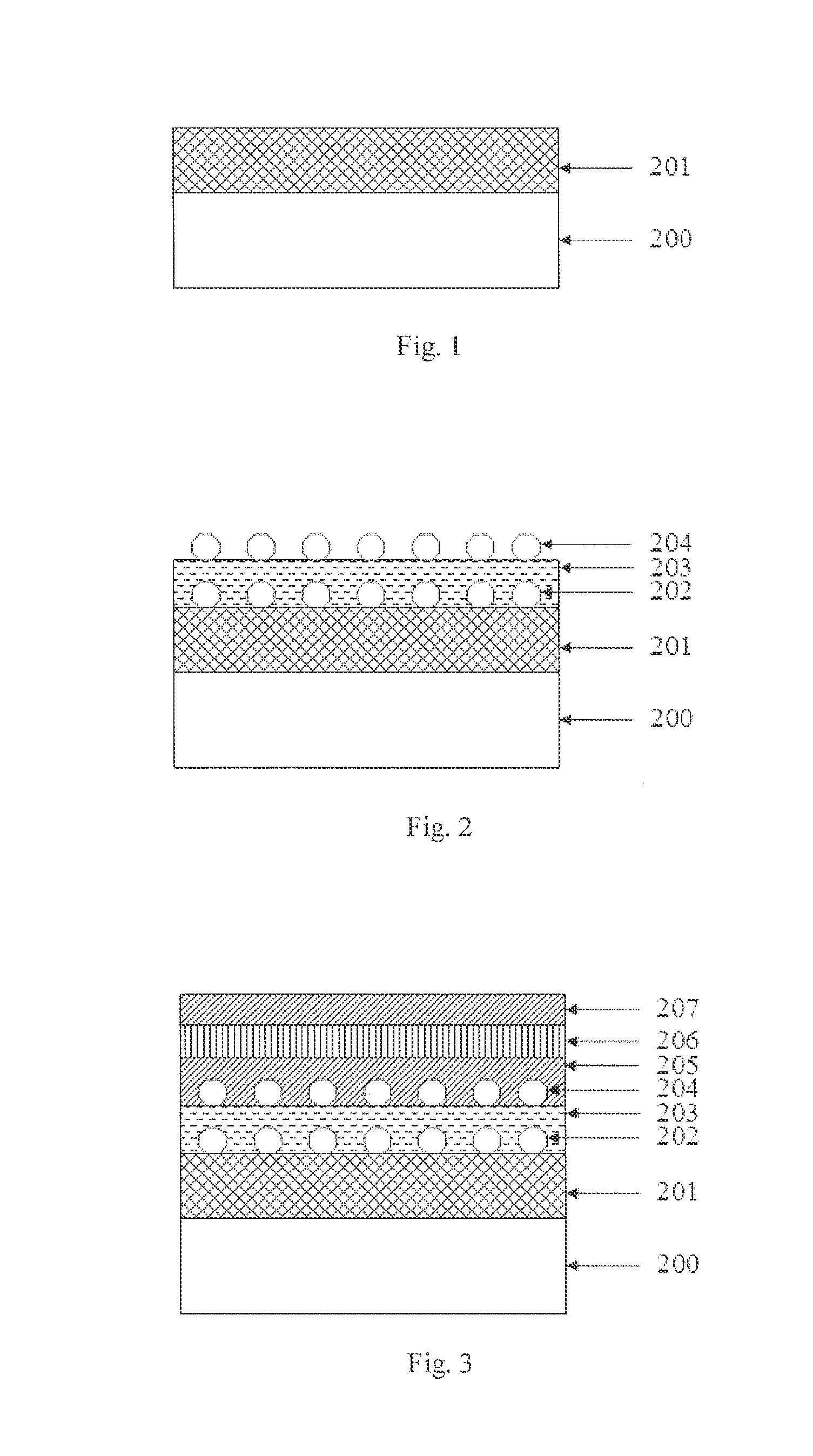
[0048]The following contents further illustrate the detailed implementation of present invention in combination with attached drawings and detailed description of the embodiments. In the FIG. enlarging or diminishing sizes of the different lavers and the area is to explain the present invention conveniently, and the shown sizes neither represent the actual sizes, nor reflect proportional relation of sizes.

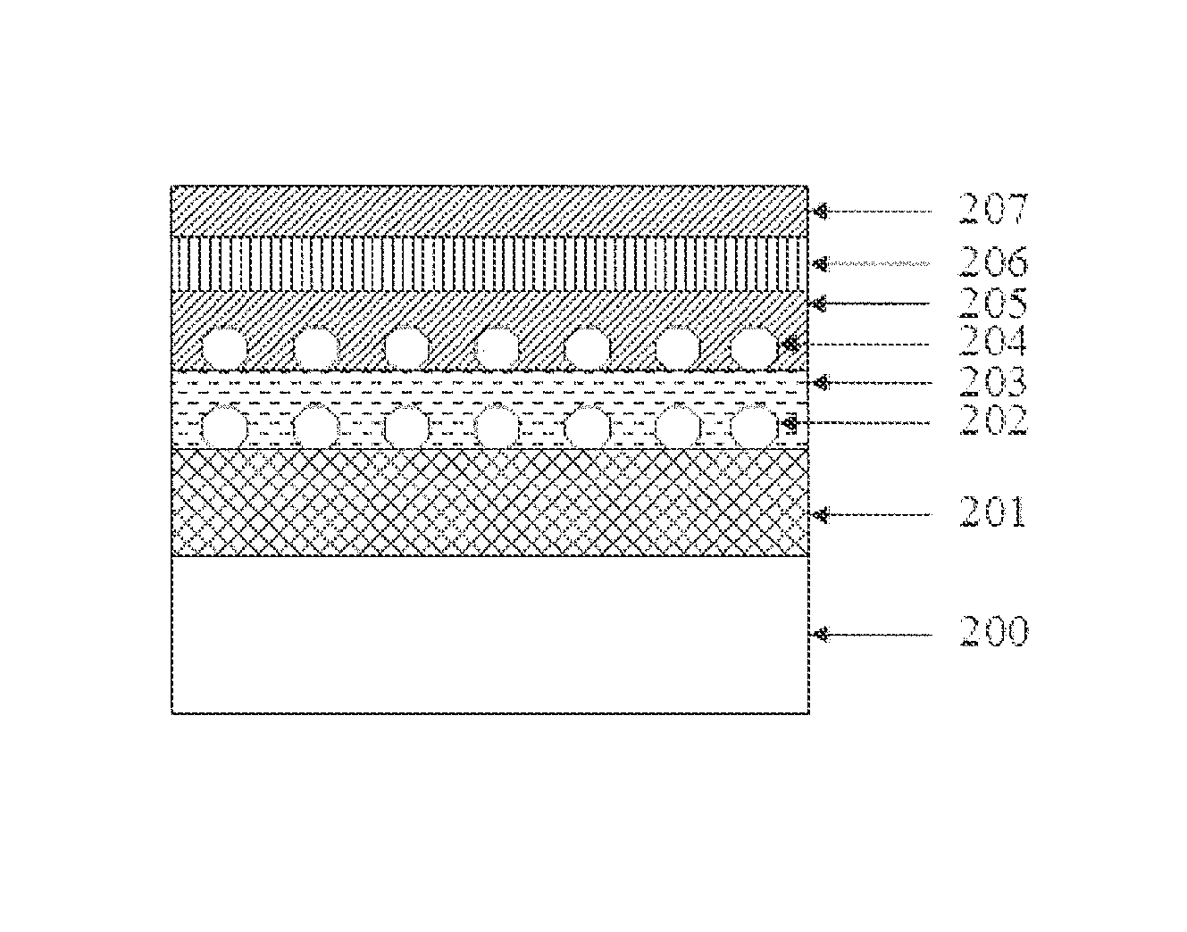
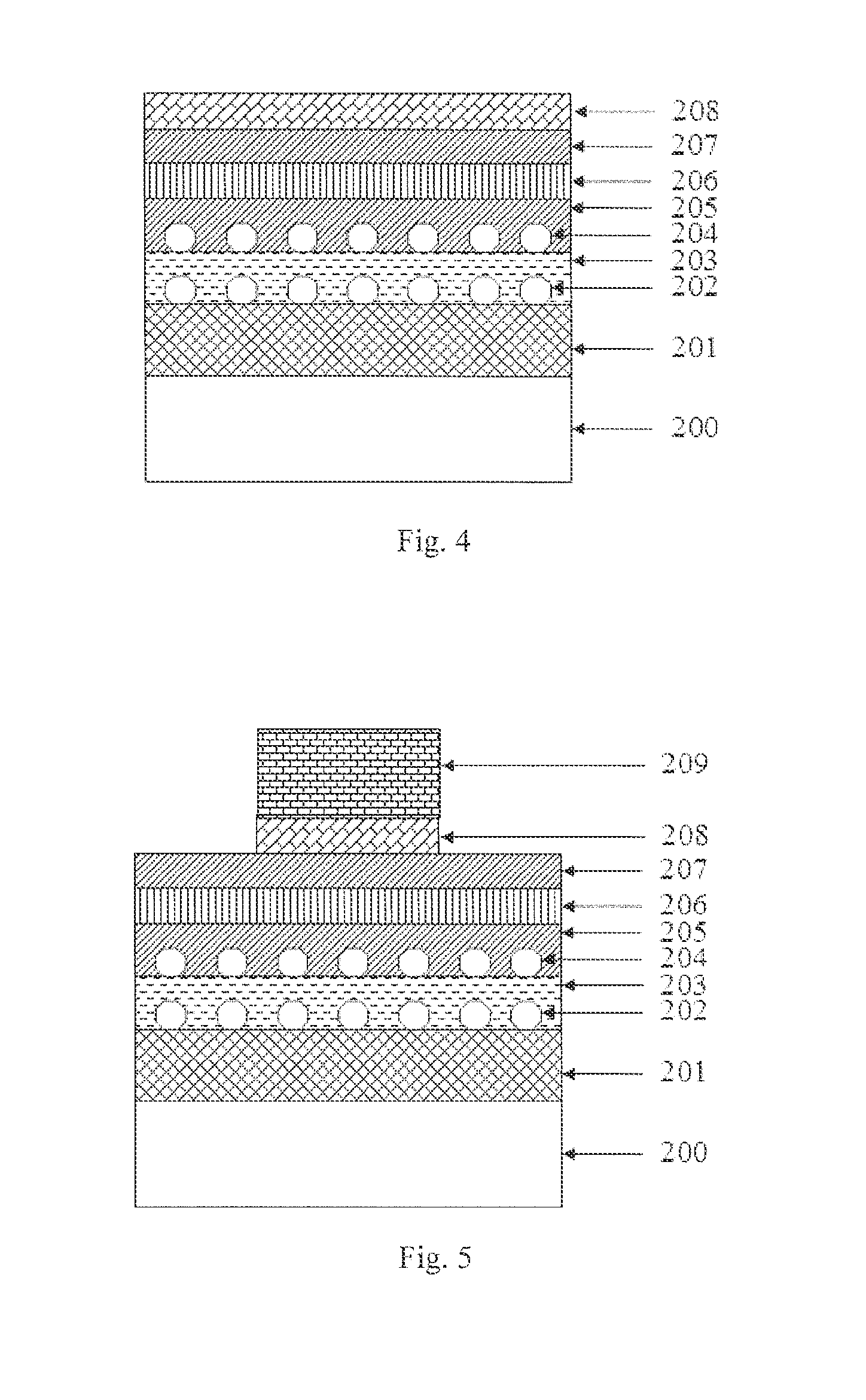
[0049]As shown in FIG. 9, it is the structure diagram of the TFT memory in this invention, the gate electrode 200 is used as the substrate, in sequence from bottom to up: charge blocking layer 201, charge storage layer which includes two-layer metal nanocrystals, charge tunneling layer with symmetrical stack structure, the active region of the device and source / drain electrodes.

[0050]The said gate electrode substrate 200 can be the heavily doped P type monocrystalline silicon wafer, heavily doped N type rnonocrystalline silicon wafer, ITO film, metal suicide film or the other mater...


PUM


Abstract

The invention relates to a thin film transistor memory and its fabricating method, This memory using the substrate as the gate electrode from bottom to up includes a charge blocking layer, a charge storage layer, a charge tunneling layer, an active region of the device and source/drain electrodes. The charge blocking layer is the ALD grown Al2O3 film. The charge storage layer is the two layer metal nanocrystals which include the first layer metal nanocrystals, the insulting layer and the second layer metal nanocrystals grown by ALD method. in sequence from bottom to up. The charge tunneling layer is the symmetrical stack layer which includes the SiO2/HfO2/SiO2 or Al2O3/HfO2/Al2O3 film grown. by ALD method in sequence from bottom to up. The active region of the device is the IGZO film grown by the RF sputtering method, and it is formed by the standard lithography and wet etch method. The TFT memory in this invention has the advantage with large P/E window, good data retention, high P/E speed, stable threshold voltage and simple fabricating process.

Description

FIELD OF INVENTION[0001]The invention relates to a semiconductor integrated circuits manufacturing technology, and, particularly to a thin film transistor memory and its fabricating method.BACKGROUND OF INVENTION[0002]Nonvolatile memory is one of the indispensable elements in modern electronic devices, but most of the nonvolatile memories in the market are still the one based on silicon substrate. However, the traditional nonvolatile floating gate memories fabricated on monocrystalline silicon substrate are difficult to fabricate on the glass substrate due to the complicated fabricating method and high process temperature, and that will lead them subject to many restrictions when they are applied on the display panel.[0003]Recently, a new nonvolatile memory based on thin film transistor (TFT) structure has aroused great attention. This type of nonvolatile memory not only can be fabricated on glass or flexible substrate but also has a good compatible with traditional TFT manufacturin...

Claims


Application Information

Patent Timeline
IPC IPC(8): H01L29/792H01L29/66
CPCH01L29/792H01L29/66742H01L29/7881H01L29/66825H01L29/66833
Inventor DING, SHIJINCHEN, SUNCUI, XINGMEIWANG, PENGFEIZHANG, WEI
Owner FUDAN UNIV
Why Eureka
Try Eureka