Large Diameter, High Quality SiC Single Crystals, Method and Apparatus

a silicon carbide and single crystal technology, applied in the direction of polycrystalline material growth, manufacturing tools, transportation and packaging, etc., can solve the problems of affecting the progress of sic-based devices, and affecting the stability of sic-based devices

Active Publication Date: 2013-10-24
II VI DELAWARE INC
View PDF3 Cites 41 Cited by
  • Summary
  • Abstract
  • Description
  • Claims
  • Application Information

AI Technical Summary

Benefits of technology

[0082]The method can further include applying electrical power to the first and second resistance heaters of a sufficient extent to raise the crucible temperature to the SiC sublimation temperature and create in the interior of the crucible temperature gradients, including: a temperature gradient in the seed compartment of the crucible, said seed compartment temperature gradient is controlled to have its radial component positive (i.e., cooler at the center of the seed compartment and hotter adjacent the wall of the crucible) and not exceeding 10 K / cm in magnitude, and a temperature gradient in the source compartment of the crucible, said source compartment temperature gradient being of sufficient magnitude to cause the initial source material to sublime and condense on the separation plate thereby forming a densified polycrystalline SiC body.
[0083]The method can further include maintaining the electrical power to the first and second resistance heaters to: cause the densified polycrystalline SiC body to sublime and generate the vapor; force the vapor generated upon sublimation of the densified polycrystalline SiC body to move across the vapor-permeable central area of the separation plate; force the vapor passed across the vapor-permeable portion of the separation plate to move to the central area of the seed and condense on said seed causing the crystal to grow; and grow the crystal to a desired size.

Problems solved by technology

However, progress in SiC-based devices is still hampered by the scarcity of commercially available, high-quality 150 mm SiC substrates and by the absence of 200 mm substrates.
Harmful defects in SiC substrates include: dislocations, micropipes, stacking faults, inclusions of foreign polytypes and carbon inclusions.
Stress in the SiC substrate is another factor detrimental to the device performance and technology.
TSDs cause leakage and device degradation, while BPDs lead to the generation of stacking faults under bias and, subsequently, to the terminal device failure.
MPs are “device killers” causing severe charge leakage even at low bias voltages.
Micropipes are “device killers” causing severe charge leakage even at low bias voltages.
Stacking faults (SFs) are two-dimensional defects violating the ideal stacking sequence and emerging as a result of non-optimized growth conditions.
Steep radial gradients cause stress and appearance of stress-related crystal defects, such as BPDs.
A strongly curved growth interface, convex or concave, leads to the appearance of crude macrosteps on the interface, stacking faults, inclusions of foreign polytypes and other defects.
A concave toward the source (hereafter ‘concave’) interface leads to the generation and rapid accumulation of various defects during growth.
The conventional, single-coil SiC sublimation growth arrangement from FIG. 1 suffers from poorly controllable radial temperature gradients, especially when the crystal diameter is large.
Disadvantages of the growth system disclosed in the '136 patent include poor coupling of the flat coils to the cylindrical crucible, while disk-shaped resistive heaters obstruct heat dissipation in the axial direction, leading to strongly negative radial gradients.
However, strongly convex isotherms and associated with them steep radial gradients cause stress and crystal defects.
Another common problem of SiC sublimation growth is carbon inclusions originating from the spent (carbonized) source.

Method used


Image

  • Large Diameter, High Quality SiC Single Crystals, Method and Apparatus
  • Large Diameter, High Quality SiC Single Crystals, Method and Apparatus
  • Large Diameter, High Quality SiC Single Crystals, Method and Apparatus

Examples


first embodiment

[0126]The principle of invention is illustrated in FIG. 5. In similarity to conventional SiC sublimation growth, cylindrical crucible 50 includes SiC seed crystal 53 disposed at the top and SiC source material 51 disposed at the bottom. The vapor flux is controlled by a plate 56 disposed in the crucible 50 in the space between the source 51 and seed crystal 53. The chemically inert separation plate 56 is impervious to the vapors 54 and has a central opening 56a. In operation, source 51 vaporizes and generates vapors 54, that migrate toward the seed 53. The opening 56a in plate 56 restricts the vapor flux by forming a vapor column 57. The vapor in column 57 migrates toward the SiC seed crystals 53 and reaches said seed substantially at the central area of the seed 53. This geometry of vapor flux creates a tendency toward convex growth interface. The remaining elements comprising a SiC sublimation growth cell (e.g., FIG. 1) that includes crucible 50 have been omitted from FIG. 5 for s...

second embodiment

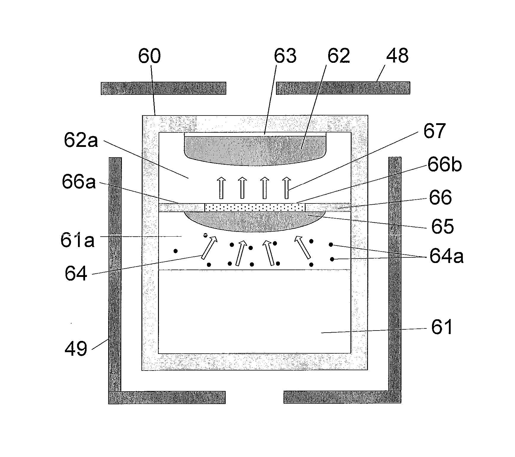
[0127]With reference to FIG. 6, a cylindrical crucible 60 is prepared of dense, fine-grain graphite, such as grade 2020 available from Mersen USA Bay City-MI Corp. 900 Harrison Street, Bay City, Mich. 48708, grade IG-11 available from Toyo Tanso USA, Inc. 2575 NW Graham Circle, Troutdale, Oreg. 97060, or similar, without limitation. Crucible 60 is loaded at the bottom with SiC source material 61, e.g., as-synthesized polycrystalline SiC grain with a particle size, desirably, between 0.1 and 2 mm. A SiC seed crystal 63 is disposed at the top of crucible 60.

[0128]FIG. 6 shows a non-limiting embodiment of the invention, wherein crucible 60 is loaded at the bottom with SiC source material 61. It is envisioned, however, that SiC source material 61 can be disposed alternatively in crucible 60, such as, without limitation, spaced at a distance from the bottom of crucible 60 or at a distance from the walls of crucible 60.

[0129]A separation plate 66 is prepared, which is chemically inert to ...


PUM

PropertyMeasurementUnit
thicknessaaaaaaaaaa
thicknessaaaaaaaaaa
areaaaaaaaaaaa

Abstract

A method and system of forming large-diameter SiC single crystals suitable for fabricating high crystal quality SiC substrates of 100, 125, 150 and 200 mm in diameter are described. The SiC single crystals are grown by a seeded sublimation technique in the presence of a shallow radial temperature gradient. During SiC sublimation growth, a flux of SiC bearing vapors filtered from carbon particulates is substantially restricted to a central area of the surface of the seed crystal by a separation plate disposed between the seed crystal and a source of the SiC bearing vapors. The separation plate includes a first, substantially vapor-permeable part surrounded by a second, substantially non vapor-permeable part. The grown crystals have a flat or slightly convex growth interface. Large-diameter SiC wafers fabricated from the grown crystals exhibit low lattice curvature and low densities of crystal defects, such as stacking faults, inclusions, micropipes and dislocations.

Description

BACKGROUND OF INVENTION[0001]1. Field of Invention[0002]The invention relates to high-quality, large-diameter silicon carbide (SiC) single crystals of 4H and 6H polytype and the sublimation growth process thereof. The SiC single crystals of invention can be used in semiconductor, electronic and optoelectronic devices, such as high power and high frequency diodes and transistors, ultra-fast semiconductor optical switches, detectors working in harsh environments and many others.[0003]The invention is an improved process of SiC sublimation crystal growth. The main novel aspect of the invention is in control of the vapor transport and temperature gradients, wherein said transport is restricted to the central area of the growing crystal, while the crystal and its environs are under conditions of near-zero radial temperature gradients. This leads to the advantageously shaped growth interface, such as flat or slightly convex towards the source, reduced crystal stress and reduced densities ...

Claims


Application Information

Patent Timeline
Patent Type & Authority Applications(United States)
IPC IPC(8): C30B23/00B28D5/00C30B29/36
CPCC30B23/005C30B29/36B28D5/00Y10T428/21C30B25/14C30B23/06
Inventor ZWIEBACK, ILYAANDERSON, THOMAS E.SOUZIS, ANDREW E.RULAND, GARY E.GUPTA, AVINASH K.RENGARAJAN, VARATHARAJANWU, PINGXU, XUEPING
Owner II VI DELAWARE INC
Why Eureka
Try Eureka