Solar cell and method of manufacture thereof, and solar cell module

Active Publication Date: 2013-11-28
KANEKA CORP
3 Cites 34 Cited by

AI-Extracted Technical Summary

Problems solved by technology

However, since conductive oxide, such as indium tin oxide (ITO) or zinc oxide, forming the transparent electrode layer has a resistivity higher than that of metal, there is such a problem that the internal resistance of the solar cell increases.
This method is simple in terms of the process itself, but has such a problem that the material co...

Benefits of technology

[0034]According to the present invention, a collecting electrode can be formed by a plating method, and therefore the collecting electrode is made less resistive, so that conversion efficiency of a solar cell can be improved. The method for forming a collecting electrode by a plating method in the p...

Abstract

Disclosed is a solar cell having a collecting electrode on one main surface of a photoelectric conversion section. The collecting electrode includes a first electroconductive layer and a second electroconductive layer in this order from the photoelectric conversion section side, and further includes an insulating layer between the first electroconductive layer and the second electroconductive layer. The first electroconductive layer includes a low-melting-point material, and a part of the second electroconductive layer is conductively connected with the first electroconductive layer through, for example, an opening in the insulating layer. The second electrode layer is preferably formed by a plating method. In addition, it is preferable that before forming the second electroconductive layer, annealing by heating is carried out to generate the opening section in the insulating layer.

Application Domain

Technology Topic

Image

  • Solar cell and method of manufacture thereof, and solar cell module
  • Solar cell and method of manufacture thereof, and solar cell module
  • Solar cell and method of manufacture thereof, and solar cell module

Examples

  • Experimental program(26)

Example

Example 1
[0136]A heterojunction solar cell of Example 1 was manufactured in the following manner.
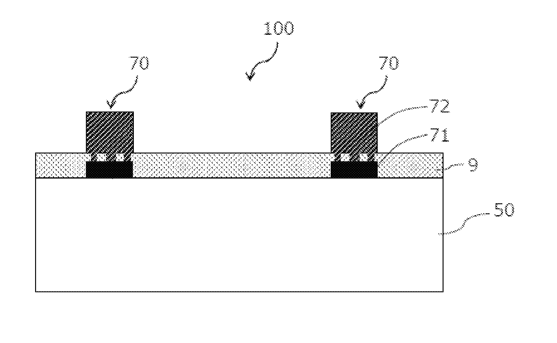
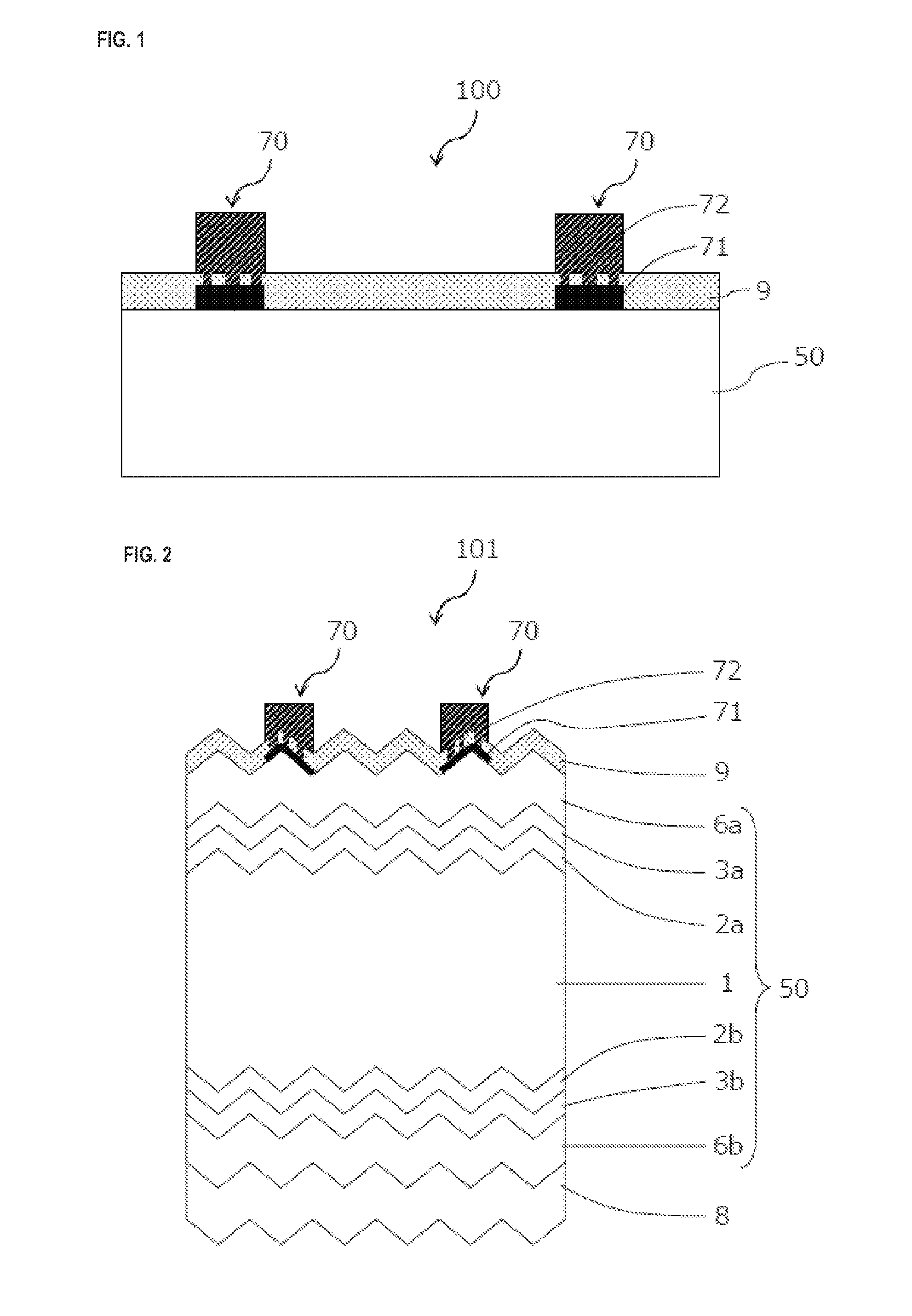
[0137]An n-type single-crystal silicon wafer having a light incident surface direction identical to the (100) surface and having a thickness of 200 μm was provided as a single-crystal silicon substrate of a first conductivity type. The silicon wafer was immersed in a 2 wt % aqueous HF solution for 3 minutes to remove silicon oxide covering on the surface, and thereafter rinsed twice with ultrapure water. The silicon substrate was immersed in a 5/15 wt % aqueous KOH/isopropyl alcohol solution held at 70° C. for 15 minutes, and the surface of the wafer was etched to form a textured surface. Thereafter, the wafer was rinsed twice with ultrapure water. The surface of the wafer was observed using an atomic force microscope (AFM manufactured by Pacific Nanotechnology, Inc.), and it was confirmed that the surface of the wafer was mostly etched, and a pyramidal texture surface exposed at the (111) plane was formed.
[0138]The wafer after etching was introduced into a CVD apparatus, and at the light incident side thereof, i-type amorphous silicon was formed with a thickness of 5 nm as an intrinsic silicon-based thin-film 2a. Conditions for forming i-type amorphous silicon included a substrate temperature of 150° C., a pressure of 120 Pa, a SiH4/H2 flow ratio of 3/10 and a power density supply of 0.011 W/cm2. The thickness of the thin-film in this example is a value calculated from a formation rate determined by measuring the thickness of a thin-film formed on a glass substrate under the same conditions using a spectroscopic ellipsometry (trade name: M2000, manufactured by J. A. Woollam Co. Inc.).
[0139]On the i-type amorphous silicon layer 2a, p-type amorphous silicon was formed with a thickness of 7 nm as a silicon-based thin-film 3a of an opposite conductivity type. Conditions for forming the p-type amorphous silicon layer 3a included a substrate temperature of 150° C., a pressure of 60 Pa, a SiH4/B2H6 flow ratio of 1/3 and a power density supply of 0.01 W/cm2. The B2H6 gas flow rate mentioned above is a flow rate of a diluting gas wherein B2H6 concentration was diluted to 5000 ppm using H2 gas.
[0140]Thereafter, on the back side of the wafer, an i-type amorphous silicon layer was formed with a thickness of 6 nm as an intrinsic silicon-based thin-film 2b. Conditions for forming the i-type amorphous silicon layer 2b were the same as those for the aforementioned i-type amorphous silicon layer 2a. On the i-type amorphous silicon layer 2b, an n-type amorphous silicon layer was formed with a thickness of 4 nm as a silicon-based thin-film 3b of the first conductivity type. Conditions for forming the n-type amorphous silicon layer 3b included a substrate temperature of 150° C., a pressure of 60 Pa, a SiH4/PH3 flow ratio of 1/2 and a power density supply of 0.01 W/cm2. The PH3 gas flow rate mentioned above is a flow rate of a diluting gas wherein PH3 concentration was diluted to 5000 ppm using H2 gas.
[0141]Indium tin oxide (ITO, refractive index: 1.9) was formed thereon with a thickness of 100 nm as transparent electrode layers 6a and 6b, respectively. The transparent electrode layer was formed by applying a power density of 0.5 W/cm2 in an argon atmosphere at a substrate temperature of room temperature and a pressure of 0.2 Pa using indium oxide as a target. On the back side transparent electrode layer 6b, silver was formed with a thickness of 500 nm as a back side metal electrode 8 by a sputtering method. A collecting electrode 7 having a first electroconductive layer 71 and a second electroconductive layer 72 was formed on the light incident side transparent electrode layer 6a in the following manner.
[0142]For formation of the first electroconductive layer 71, a printing paste containing SnBi metal powder (particle size DL=25 to 35 μm; melting point T1=141° C.) as a low-melting-point material and a silver powder (particle size DH=2 to 3 μm; melting point T2=971° C.) as a high melting-point material at a weight ratio of 20:80, and further containing an epoxy-based resin as a binder resin was used. The printing paste was screen-printed using a screen plate of #230 mesh (opening width: 1=85 μm) having an opening width (L=80 μm) matching a collecting electrode pattern, and dried at 90° C.
[0143]The wafer with the first electroconductive layer 71 formed thereon was introduced into a CVD apparatus, and a silicon oxide layer (refractive index: 1.5) was formed on the light incident surface side with a thickness of 80 nm as an insulating layer 9 by a plasma-enhanced CVD method.
[0144]Conditions for forming the insulating layer 9 included a substrate temperature of 135° C., a pressure of 133 Pa, a SiH4/CO2 flow ratio of 1/20 and a power density supply of 0.05 W/cm2 (frequency 13.56 MHz). The refractive index (n) and extinction coefficient (k) of the insulating layer formed on the light incident side under the conditions were as shown FIG. 10. Thereafter, the wafer after formation of the insulating layer was introduced into a circulating hot air oven, and subjected to an annealing treatment at 180° C. for 20 minutes in an air atmosphere.
[0145]The substrate 12 subjected to steps up to and including the annealing step as described above was introduced into a plating tank 11 as shown in FIG. 7. For a plating solution 16, one obtained by adding additives (product numbers: ESY-2B, ESY-H and ESY-1A, manufactured by Uyemura & CO., LTD.) to a solution prepared so that the concentrations of copper sulfate pentahydrate, sulfuric acid and sodium chloride were 120 g/l, 150 g/l and 70 mg/l, respectively, was used. Using the plating solution, plating was carried out under conditions including a temperature of 40° C. and a current of 3 A/dm2, so that on the insulating layer on the first electroconductive layer 71, copper was uniformly deposited at a thickness of about 10 μm as a second electroconductive layer 72. Little copper was deposited onto a region where no first electroconductive layer was formed.
[0146]Thereafter, the silicon wafer on the cell outer periphery was removed in a width of 0.5 mm by a laser processing apparatus to prepare the heterojunction solar cell of the present invention.

Example

Examples 2 to 4
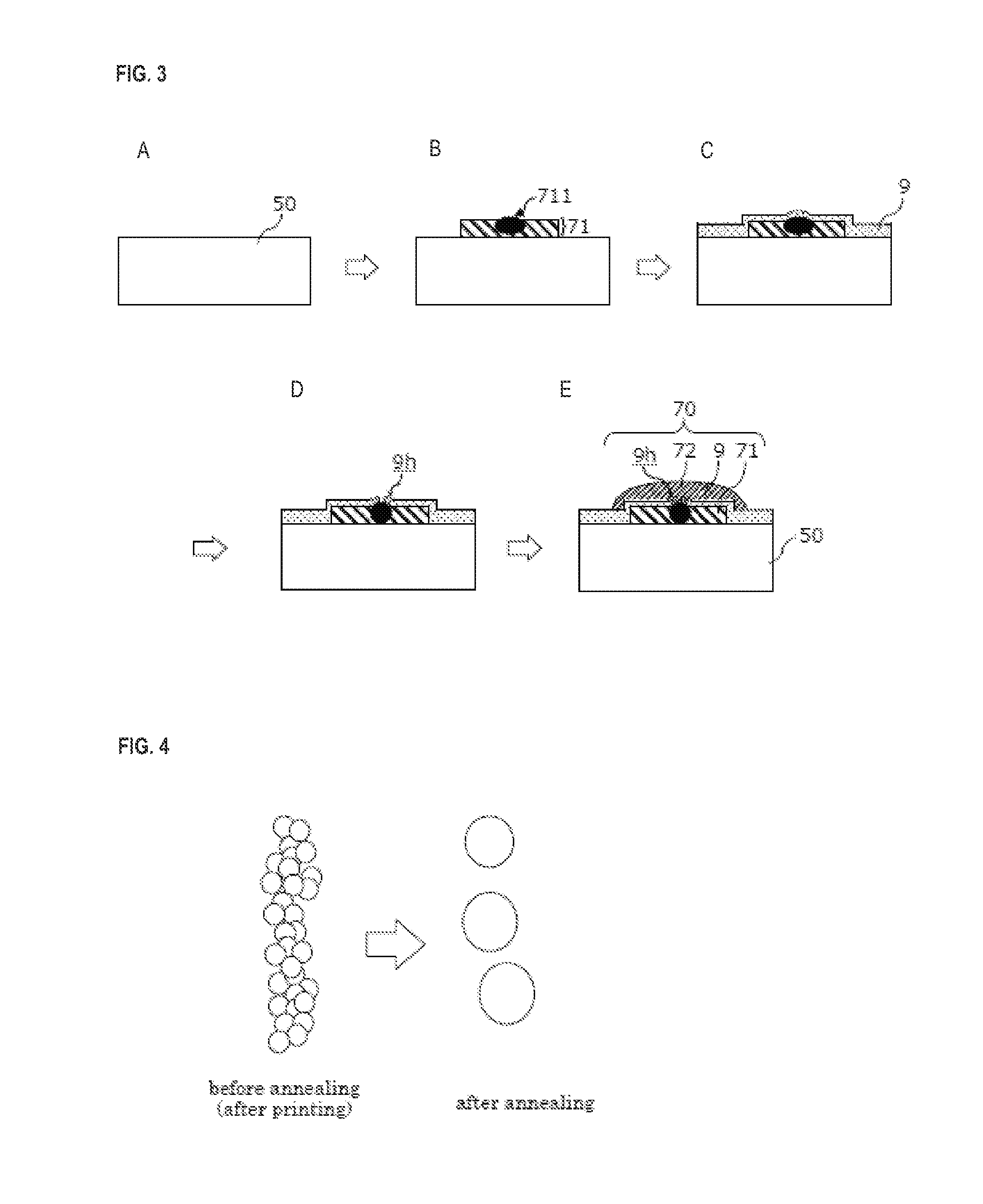
[0147]A heterojunction solar cell was prepared in the same manner as in Example 1 except that the ratio of a metallic material powder to a silver powder in the printing paste for forming the first electroconductive layer 71 was changed as shown in Table 1.

Example

Examples 5 and 6
[0148]A heterojunction solar cell was prepared in the same manner as in Example 1 except that the thickness of the insulating layer 9 was changed as shown in Table 1.

PUM

no PUM

Description & Claims & Application Information

We can also present the details of the Description, Claims and Application information to help users get a comprehensive understanding of the technical details of the patent, such as background art, summary of invention, brief description of drawings, description of embodiments, and other original content. On the other hand, users can also determine the specific scope of protection of the technology through the list of claims; as well as understand the changes in the life cycle of the technology with the presentation of the patent timeline. Login to view more.

Similar technology patents

Display panel and manufacturing method thereof

ActiveUS10943956B2Conversion efficiency be improveSolid-state devicesDiodePhysicsOptical path
Owner:SHENZHEN CHINA STAR OPTOELECTRONICS SEMICON DISPLAY TECH CO LTD

Solar Cell

InactiveUS20110253204A1Conversion efficiency be improveSolid-state devicesPhotovoltaic energy generationSolar cellP–n junction
Owner:RIKEN

Classification and recommendation of technical efficacy words

  • High efficiency
  • Conversion efficiency be improve

Antenna and communication device

InactiveUS20050116861A1Easy to handleConversion efficiency be improveSimultaneous aerial operationsAntenna supports/mountingsMonopole antennaCarbon nanotube
Owner:FUJIFILM BUSINESS INNOVATION CORP

Organic solar cell and method of fabricating the same

InactiveUS20100326524A1Photocurrent be increaseConversion efficiency be improveSolid-state devicesSemiconductor/solid-state device manufacturingBlock layerElectron blocking layer
Owner:SAMSUNG ELECTRONICS CO LTD

Nanowire thermoelectric device

ActiveUS20100147350A1Conversion efficiency be improveReduce thermal resistance lossThermoelectric device with peltier/seeback effectThermoelectric device junction materialsElectrically conductiveElectric energy
Owner:IND TECH RES INST

Switching power supply device

Owner:FUJI ELECTRIC CO LTD
Why Eureka
Try Eureka