Magnetic Tunnel Junction Device Having Amorphous Buffer Layers That Are Magnetically Connected Together And That Have Perpendicular Magnetic Anisotropy

a tunnel junction and buffer layer technology, applied in the field of magnetic tunnel junction devices, can solve the problems of deterioration of tunnel insulating layer, and many limitations in the uniformity of magnetoresistance, so as to achieve significant improvement of magnetic tunnel junction device characteristics and uniformity of magnetoresistance.

Active Publication Date: 2013-11-28
SAMSUNG ELECTRONICS CO LTD
View PDF9 Cites 49 Cited by
  • Summary
  • Abstract
  • Description
  • Claims
  • Application Information

AI Technical Summary

Benefits of technology

[0026]In the case that a magnetic tunnel junction device is fabricated according to a first embodiment of the present invention, since the non-uniformity of a tunnel insulating layer that may occur during a heat treatment process may be improved and the diffusion of antiferromagnetic particles that may be formed under a pinned layer may be prevented, the uniformity of magnetoresistance may be improved. As a result, characteristics of the magnetic tunnel junction device may be significantly improved.
[0027]Also, according to a second embodiment of the present invention, as a result of inserting a FeZr monolayer as a thin amorphous buffer layer, it may be confirmed that perpendicular magnetic anisotropy occurs in a CoFeB layer adjacent to an Mg0 layer after a heat treatment.
[0028]Since the buffer layer is thin, damage to a sample, which may occur in a prolonged etching process due to the u...

Problems solved by technology

However, with respect to a typical magnetic tunnel junction device, many limitations in the uniformity of magnetoresistance have been reported.
That is, the flatness of the tunnel insulating layer may be deteriorated due to a lower structure of the tunnel insulating layer during the heat treatment process.
However, since the lower structure may become rough as the lower structure of the tunnel insulating layer is crystallized, the tunnel insulating layer formed on the lower structure is affected thereby, and thus, the flatness of the tunnel insulating layer deteriorates.
As a result, according to a typical structure, since the characteristics of each magnetic tunnel junction device may be different even in the case in which each magnetic tunnel junction device is formed on the same wafer, the uniformity of magnetoresistance may not be secured.
Also, in a typical magnetic tunnel junction device, the tunnel insulating layer may be contaminated by the lower structure during the h...

Method used


Image

  • Magnetic Tunnel Junction Device Having Amorphous Buffer Layers That Are Magnetically Connected Together And That Have Perpendicular Magnetic Anisotropy
  • Magnetic Tunnel Junction Device Having Amorphous Buffer Layers That Are Magnetically Connected Together And That Have Perpendicular Magnetic Anisotropy
  • Magnetic Tunnel Junction Device Having Amorphous Buffer Layers That Are Magnetically Connected Together And That Have Perpendicular Magnetic Anisotropy

Examples


first embodiment

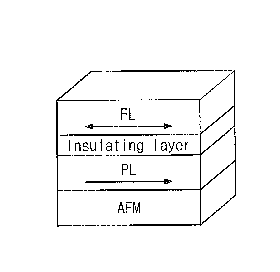
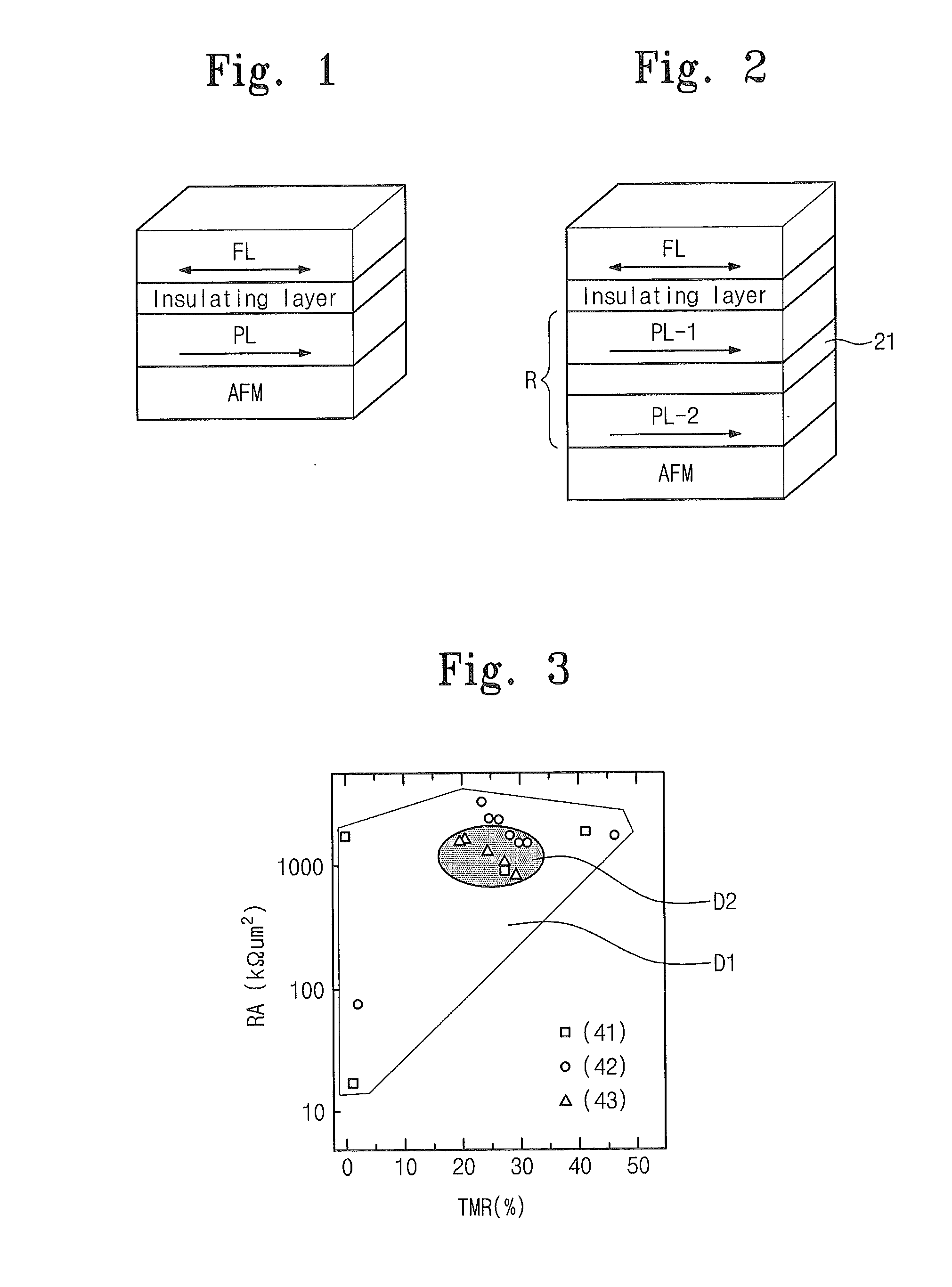
[0048]FIG. 2 is a schematic view illustrating a structure of a magnetic tunnel junction device proposed according to the present invention. For convenience in description, FIG. 2 is illustrated by focusing on a ferromagnetic layer and an AFM layer.

[0049]As described above, the magnetic tunnel junction device basically has a structure of “ferromagnetic material-insulating layer-ferromagnetic material”, and is formed in such a manner that, for convenience in operation, magnetization of one of two ferromagnetic materials is pinned and the magnetization of the other material may be varied. For convenience, the former is denoted as a pinned layer and the latter is denoted as a free layer. Since a tunneling current may vary according to whether magnetization directions of the two ferromagnetic materials are parallel or antiparallel, the magnetic tunnel junction device may function as a memory device by sensing the tunnel current.

[0050]Herein, a material that may secure a high magnetoresis...

second embodiment

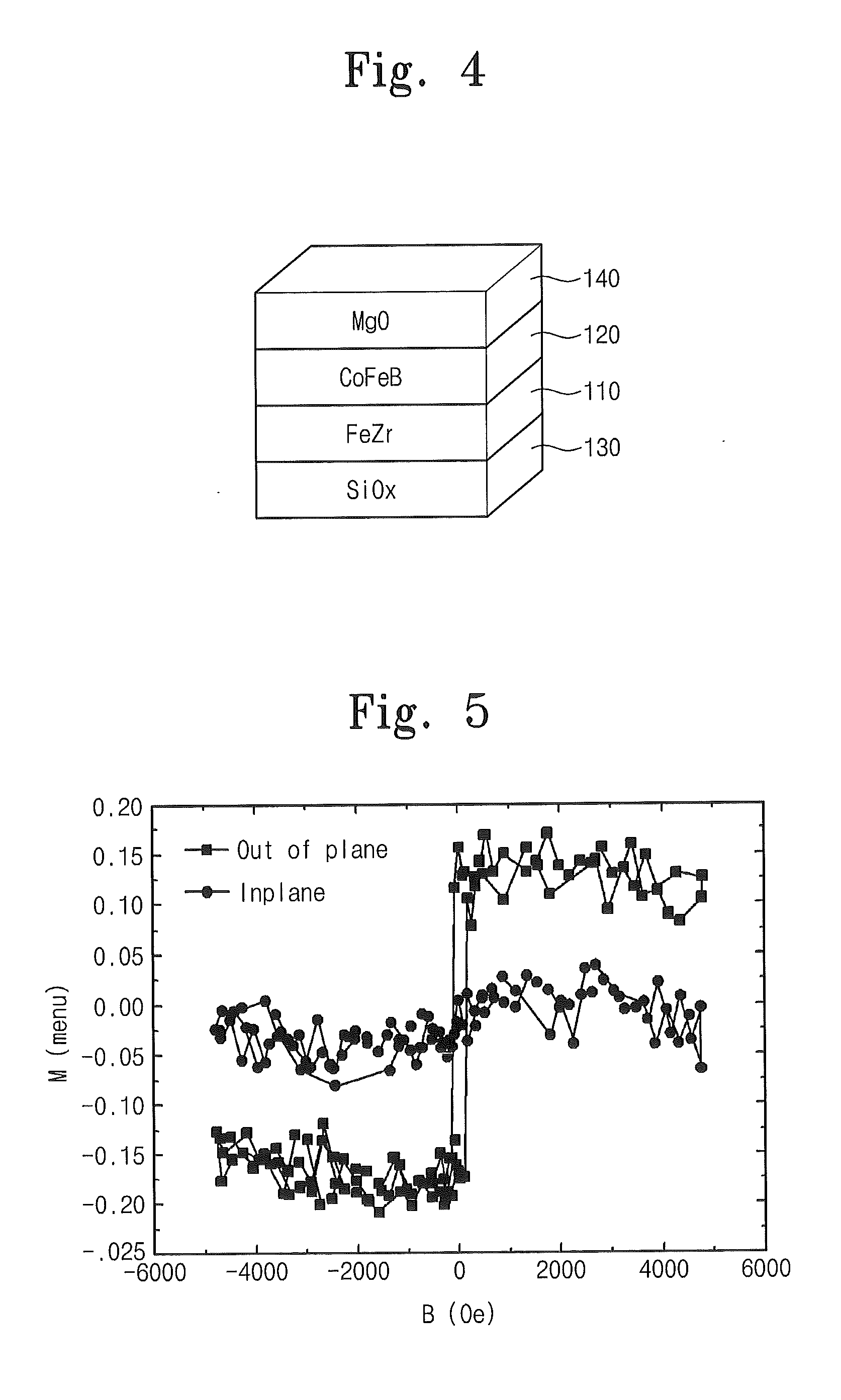
[0073]FIG. 4 is a schematic cross-sectional view illustrating an example of a magnetic device according to the present invention. In FIG. 4, in order for a CoFeB magnetic material generally having horizontal magnetic anisotropy to have perpendicular magnetic anisotropy, a stack structure of a sample is illustrated, in which perpendicular magnetic anisotropy is obtained by using a FeZr amorphous morphology buffer layer.

[0074]Herein, the expression “morphology buffer layer” denotes a layer preventing the occurrence of texture collision due to the propagation of texture into above and below adjacent thin film layers or a layer blocking the unwanted propagation of texture.

[0075]In FIG. 4, the magnetic device includes an amorphous material layer 110 and a perpendicular magnetic anisotropy material layer 120 formed on the amorphous material layer 110. The amorphous material layer 110, as a layer of a predetermined amorphous material, is formed on a bottom layer 130, and the perpendicular ...


PUM


Abstract

According to a first embodiment of the present invention, a magnetic tunnel junction device comprises: a free layer having a magnetization in a variable direction; a pinned layer having a magnetization in a pinned direction; and a tunnel insulation film formed between the free layer and the pinned layer, wherein the pinned layer includes a ferromagnetic film and an amorphous metal film. In addition, a magnetic device according to a second embodiment of the present invention comprises: an amorphous or nanocrystal material layer; and a perpendicular magnetic anisotropic material layer formed on the amorphous or nanocrystal material layer. The amorphous or nanocrystal material layer is a predefined amorphous material or nanocrystal material layer serving as a lower layer, and the perpendicular magnetic anisotropic material layer is formed on the amorphous or nanocrystal material layer.

Description

TECHNICAL FIELD[0001]The present invention relates to a magnetic tunnel junction device, and more particularly, to a magnetic tunnel junction device including a pinned layer having an amorphous metal layer, and a micro magnetic device using a perpendicular magnetic anisotropy material.BACKGROUND ART[0002]The possibility of industrial applications of spintronics has been focused since the mid-1990s. Herein, the spintronics denotes a compound word of “spin and electronics”. That is, electronics research into techniques using “electric charge”, one of two characteristics of an electron, has been mainly conducted. However, current electronics research has been conducted to develop devices having new functions by using “spin”, i.e., the other characteristics of the electron.[0003]The best way to utilize the spin of an electron is using a ferromagnetic material. In particular, magnetic tunnel junction (MTJ) device using a tunneling magnetoresistance (TMR) structure recently has received m...

Claims


Application Information

Patent Timeline
IPC IPC(8): H01L43/10
CPCH01L43/10G11C11/161H10N50/10B82Y25/00H10B61/00H10N50/85G11C11/16
Inventor RHIE, KUNGWONHONG, JINKIJUNG, KU-YOULKIM, JONGHYUN
Owner SAMSUNG ELECTRONICS CO LTD
Why Eureka
Try Eureka