
Process for manufacturing gas permeation barrier material and structure

a technology of gas permeation barrier and manufacturing process, which is applied in the field of barrier materials, can solve the problems of unacceptably degrading device performance, affecting the performance of electronic devices, and still far short of the far more challenging requirements of electronic devices

Inactive Publication Date: 2013-12-19
EI DU PONT DE NEMOURS & CO
View PDF2 Cites 34 Cited by
  • Summary
  • Abstract
  • Description
  • Claims
  • Application Information

AI Technical Summary

Benefits of technology

The present invention provides a composition of matter that is an alloy of an inorganic substance and a metalcone that are polymerically linked. The inorganic substance can be an oxide or nitride of an element of Groups IVB, IVA, VIB, IIIA, or IVA of the Periodic Table. The metalcone can be an aluminum, zincone, titanium, or zircone. The invention also provides a barrier substrate comprising the alloy and a process for manufacturing the alloy and barrier substrate. The technical effect of the invention is to provide a new material that can be used in various electronic devices, such as semiconductors, sensors, and displays, as a barrier coating to improve their performance and reliability.

Problems solved by technology

While this modest improvement is a reasonable compromise between better properties and cost for many high-volume packaging applications, the protection afforded still falls far short of the far more challenging requirements for many electronic devices.
On the other hand, electronic articles must operate satisfactorily over the entire useful life of the product, which is often an order of magnitude longer or more.
In most instances, the electronic devices use materials that react with water and / or oxygen; exposure to these contaminants can unacceptably degrade device performance.
While known inorganic coatings provide some reduction of the permeability, the levels typically attained are still inadequate.
However, the practical reality is that even elimination of obvious macroscopic defects such as pinholes that arise either from the coating process or from substrate imperfections, is still not enough to provide protection sufficient to maintain the desired device performance in practical devices.
For example, it is known that even microscopic cracks in a coating compromise its protective ability, providing a facile pathway for ambient gases to intrude.
Such cracks can arise either during coating formation or thereafter.
The PVD method is known to be particularly prone to creation of columnar microstructures having grain boundaries and other comparable defects, along which gas permeation can be especially facile.
Without adequate protection, device performance may degrade rapidly.
Moisture sensitivity is an issue for all these technologies, but is particularly acute for CIGS-based PV cells.
In addition, flexible substrates potentially would also reduce the overall device thickness.
However, substrate flexure inherently imposes stress on any coating layer.
If strain limits are exceeded, the coating may crack, likely compromising any barrier properties the coating provides, as the cracks create a facile diffusion pathway for contaminants to intrude, potentially causing device failure.
Nevertheless, none of the coatings proposed heretofore has alleviated all the detriments.

Method used


Image

  • Process for manufacturing gas permeation barrier material and structure
  • Process for manufacturing gas permeation barrier material and structure
  • Process for manufacturing gas permeation barrier material and structure

Examples


example 1

Alloy Fabrication and Water Vapor Transmission Measurements

[0103]In accordance with the present disclosure, alumina / alucone alloy films were grown on 100 mm diameter disks of 50-μm thick, flexible Kapton® EZ polyimide (available from DuPont, Wilmington, Del.) as a substrate.

[0104]The polyimide disks were affixed to conventional 4-inch diameter Si wafers and located in a hot-wall, viscous flow reactor. TMA (97%, Sigma Aldrich), EG (Reagent Plus >99%, Sigma Aldrich), and water (HPLC grade, Fisher Scientific) were used. Ultrahigh purity N2 (Airgas) was used as the carrier gas and the purge between reactant exposures. The baseline reactor pressure was 600 mTorr (80 Pa) with N2 flowing through the reactor. The substrate maintained at 135° C.

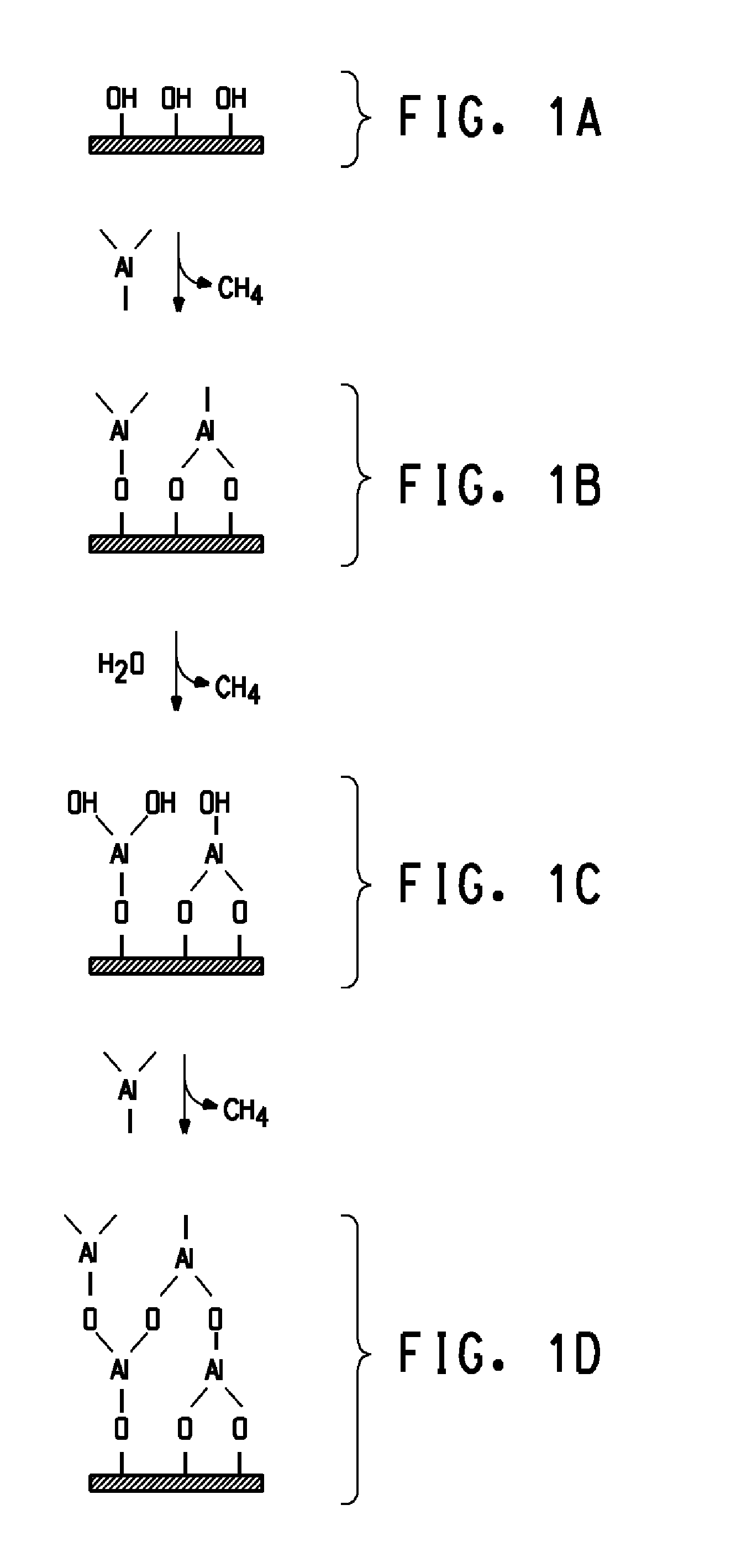
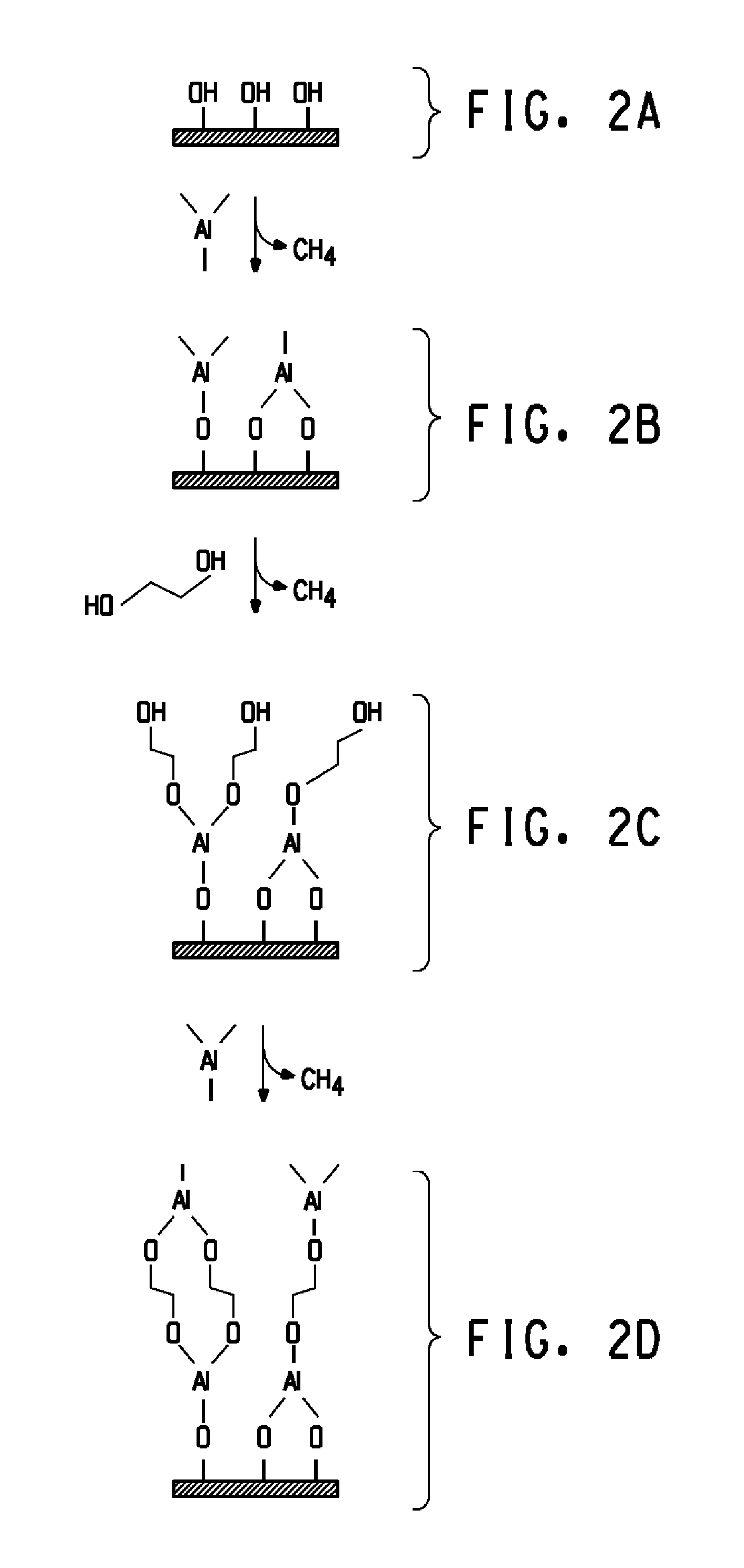
[0105]The film was formed by alternating deposition sequences of TMA / H2O for ALD deposition of alumina and TMA / EG for MLD deposition of alucone. Different alloy compositions were obtained by varying the number of ALD deposition cycles in each ALD depo...

example 2

Alloy Fabrication and Water Vapor Transmission Measurements

[0110]In accordance with the present disclosure, alumina / zircone alloy films are grown on 100 mm diameter disks of 50-μm thick, flexible Kapton® EZ polyimide (available from DuPont, Wilmington, Del.) as a substrate. Except as noted, the depositions are carried out using the same techniques employed for the samples of Example 1 above.

[0111]The MLD deposition of zircone is carried out using zirconium(IV) tert-butoxide having the chemical formula Zr[OC(CH3)3]4 and EG as the reactants. Different alloy compositions are obtained by varying the number of ALD deposition cycles in each ALD deposition sequence from 2 to 7, while each MLD deposition sequence comprised either one or two MLD cycles. The resulting films are denoted by the ratio of ALD to MLD cycles, wherein “n:m” represents a process in which each ALD deposition sequence includes “n” ALD cycles (n=2 to 7) and “m” MLD cycles (m=1 or 2). The ALD and MLD deposition sequences...

example 3

Alloy Fabrication and Critical Tensile Strain Measurements

[0114]Films for tensile testing are deposited on 75-μm thick polyimide substrates obtained from CS Hyde Company, Inc., Lake Villa, Ill. Samples are cut into rectangles of 100 mm×10 mm and then placed in the same hot-wall, viscous flow reactor used for the experiments of Example 1. The same deposition protocol is used to prepare 100 nm thick films having 1:1, 3:1 and 6:1 alumina / alucone alloy compositions. Pure alumina and alucone films are also made using the same process, but without alternating ALD and MLD deposition sequences.

[0115]Tensile testing is carried out using an Insight 2 mechanical load-frame (MTS Systems Corp., Eden Prairie, Minn.). The coated samples are tensioned at room temperature (25° C.) to a prescribed strain, which is measured using a model LE-05 laser extensometer (Electronic Instrument Research Corp., Irwin, Pa.).

[0116]After the tensioning, the samples are then inspected for the presence of cracks usin...


PUM

PropertyMeasurementUnit
Temperatureaaaaaaaaaa
Timeaaaaaaaaaa

Abstract

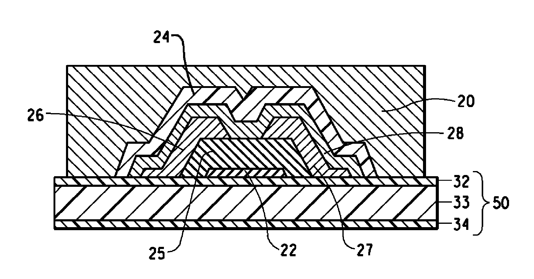
Hybrid inorganic-organic, polymeric alloys are prepared by combining atomic layer deposition and molecular layer deposition techniques provide barrier protection against intrusion of atmospheric gases such as oxygen and water vapor. The alloy may be formed either directly on objects to be protected, or on a carrier substrate to form a barrier structure that subsequently may be employed to protect an object. The alloy thus formed is beneficially employed in constructing electronic devices such as photovoltaic cell arrays, organic light-emitting devices, and other optoelectronic devices.

Description

CROSS-REFERENCE TO RELATED APPLICATIONS[0001]This application is related to a co-pending application entitled “Gas Permeation Barrier Material” and bearing attorney docket number CL5414 US-NP; and a co-pending application entitled “Electronic Device With Gas Permeation Barrier Protective Coating” and bearing attorney docket number CL5767 US-NP, said applications being filed of even date herewith by the same inventors. Each of these applications is incorporated herein in its entirety for all purposes by reference thereto.FIELD OF THE INVENTION[0002]This invention relates to a barrier material, and more particularly, to a process for manufacturing hybrid inorganic-organic polymeric gas permeation barrier materials, structures and devices made therewith.BACKGROUND[0003]A wide variety of industrial and commercial products and devices require some level of protection from ambient oxygen and / or water vapor to prevent degradation or failure. Some items can readily be sealed within a rigid,...

Claims


Application Information

Patent Timeline
IPC IPC(8): C23C16/06C23C16/38B32B37/00C23C16/40
CPCB32B2037/246B32B2457/12B32B2457/206C23C16/403C23C16/45527Y02E10/549Y10T156/10Y02P70/50H10K10/88H10K30/88H10K59/8722H10K59/873H10K50/844
Inventor CARCIA, PETER FRANCISMCLEAN, ROBERT SCOTT
Owner EI DU PONT DE NEMOURS & CO
Learn More