Zinc oxide-based sputtering target, method of manufacturing the same, and thin-film transistor having barrier layer deposited using the same

Inactive Publication Date: 2013-12-26
SAMSUNG DISPLAY CO LTD +2
View PDF0 Cites 15 Cited by
  • Summary
  • Abstract
  • Description
  • Claims
  • Application Information

AI Technical Summary

Benefits of technology

[0033]According to embodiments of the present invention, it is possible to manufacture a high-density sputtering target that can be reliably subjected to DC sputtering by doping zinc oxide with gallium oxide.
[0034]In addition, during manufacturing of the TFT, when an oxide protective layer based on SiOx is deposited on the gate, source and drain electrodes which can be made of Cu using the sputtering target, it is possible to prevent CuOx from forming, thereby improving the contact characteristics between the Cu electrode and the protective layer. A barrier layer that is applicable to displays but has a high transmittance can be deposited on the Cu electrode, i.e. be formed between the Cu electrode and th

Problems solved by technology

This consequently deteriorates the performance of the TFT, which is problematic.
In particular, during deposition of a protective layer that is referred to as passivation on the source and drain electrodes,

Method used


Image

  • Zinc oxide-based sputtering target, method of manufacturing the same, and thin-film transistor having barrier layer deposited using the same
  • Zinc oxide-based sputtering target, method of manufacturing the same, and thin-film transistor having barrier layer deposited using the same
  • Zinc oxide-based sputtering target, method of manufacturing the same, and thin-film transistor having barrier layer deposited using the same

Examples


Example

Example 1

[0065]Gallium oxide having an average particle diameter of 4 μm was added at a content of 20 weight percent of a sputtering target to distilled water to which a dispersing agent was added at a content of 1.0 weight percent of the gallium oxide. The resultant mixture was ground / dispersed by wet milling such that the average diameter of dispersed particles became 0.3 μm. After that, indium oxide having an average particle diameter of 0.5 μm and a dispersing agent having a content of 0.5 weight percent of the zinc oxide were added, and the resultant mixture was wet-milled such that the final diameter of dispersed particles became 0.2 μm. The dispersing agent that was used here is polyacrylic acid amine salt. After the final zinc oxide-based slurry mixture was produced, 1.0 weight percent of polyvinyl acetate (PVA) and 0.5 weight percent of polyethylene glycol (PEG) were added as a binder. Milling was carried out once again, thereby producing a uniform slurry. Afterwards, the s...

Example

Example 2

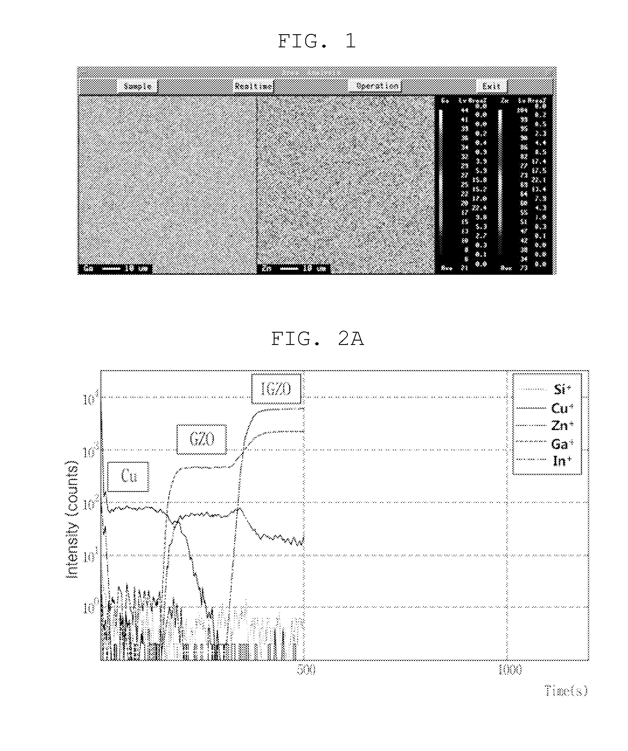
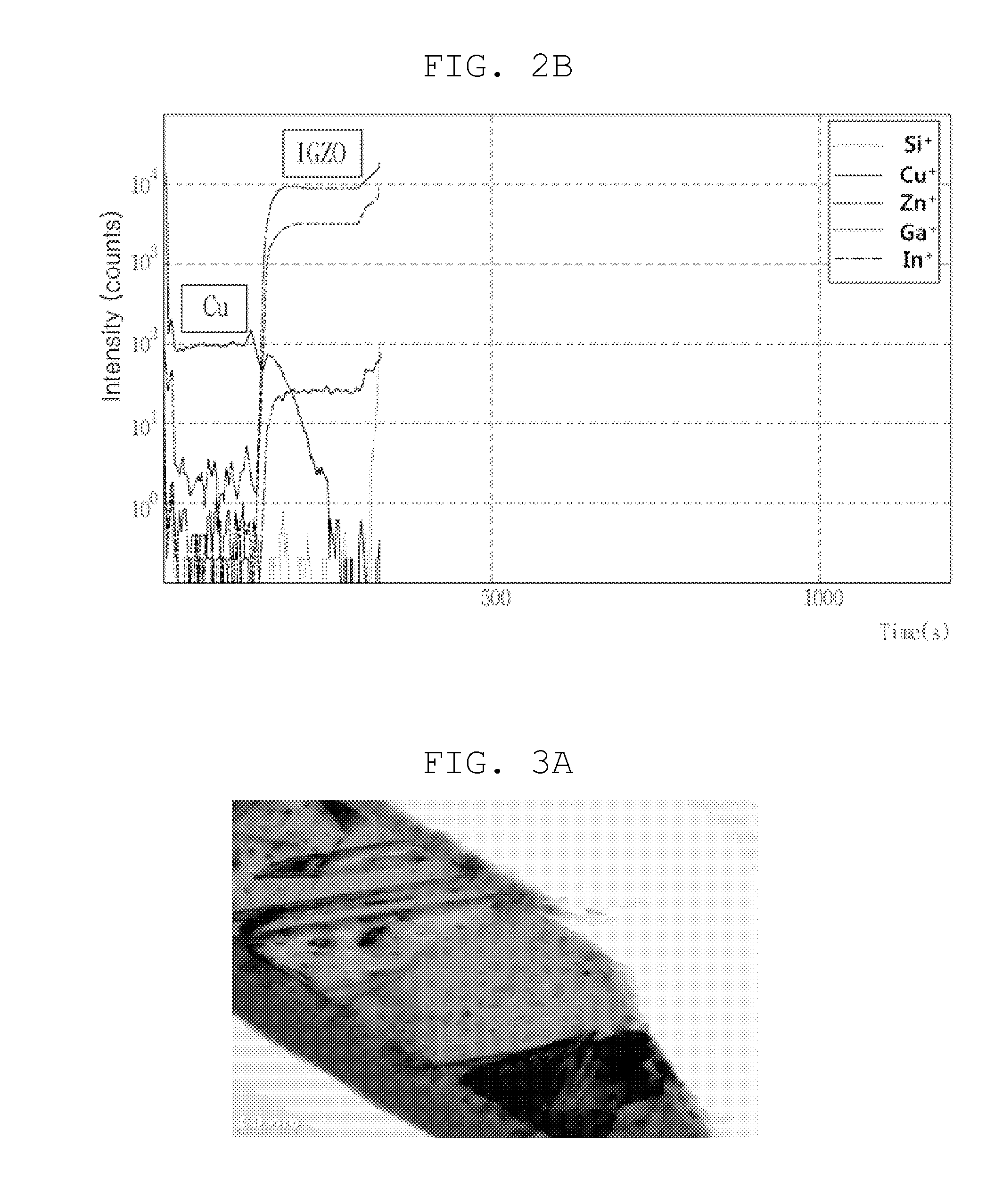
[0067]The sinter manufactured according to Example 1 was bonded to a backing plate made of Cu, and sputtering was carried out using the resultant structure. The sputtering conditions were controlled such that the base pressure of the chamber was 1×10⁻⁶ torr and the working pressure was 0.5 Pa. Deposition was enabled by causing plasma discharge at 100° C. in a pure Ar atmosphere. Here, the target size was 565 mm×690 mm, and the induced power was DC 10 kW. A resultant thin film was deposited to a thickness of 30 nm on a substrate. The substrate on which the thin film was deposited was a glass substrate that includes a piece of non-alkaline glass and an indium gallium zinc oxide (IGZO) layer which was formed on the glass in advance. Sample (a) was prepared by depositing Cu, or an electrode material, on the gallium-doped zinc oxide (GZO) thin film which was deposited at the 30 nm thickness on the IGZO layer, whereas Sample (b) was prepared by depositing Cu on the IGZO layer. A ...


PUM

PropertyMeasurementUnit
Temperatureaaaaaaaaaa
Fractionaaaaaaaaaa
Fractionaaaaaaaaaa

Abstract

A zinc oxide (ZnO)-based sputtering target, a method of manufacturing the same, and a thin-film transistor (TFT) having a barrier layer deposited using the same. The zinc oxide-based sputtering target includes a sinter containing zinc oxide doped with gallium oxide, the content of the gallium oxide ranging, by weight, from 10 to 50 percent of the sinter, and a backing plate bonded to the rear surface of the sinter to support the sinter. The zinc oxide-based sputtering target can be subjected to direct current (DC) sputtering, and improve the contact and etching characteristics of a barrier layer that is deposited using the same.

Description

CROSS REFERENCE TO RELATED APPLICATION[0001]The present application claims priority from Korean Patent Application Number 10-2012-0068354 and 10-2012-0155995 filed on Jun. 26, 2012 and Dec. 28, 2012, the entire contents of which are incorporated herein for all purposes by this reference.BACKGROUND OF THE INVENTION[0002]1. Field of the Invention[0003]The present invention relates to a zinc oxide (ZnO)-based sputtering target, a method of manufacturing the same, and a thin-film transistor (TFT) having a barrier layer deposited using the same, and more particularly, to a zinc oxide-based sputtering target which can be subjected to direct current (DC) sputtering and improve the contact and etching characteristics of a barrier layer that is deposited using the same, a method of manufacturing the same, and a TFT having a barrier layer deposited using the same.[0004]2. Description of Related Art[0005]A liquid crystal display (LCD) or an electroluminescent display (EL) has superior displayi...

Claims


Application Information

Patent Timeline
IPC IPC(8): C23C14/08C23C14/34
CPCC23C14/086C23C14/3414C23C14/34
Inventor PARK, JAEWOOKIM, DONGJOKIM, DO-HYUNJEON, WOO-SEOKPARK, JUOKSOHN, INSUNGYOON, SANGWONLEE, GUNHYOLEE, YONGJINLEE, YOONGYU
Owner SAMSUNG DISPLAY CO LTD
Why Eureka
Try Eureka