Switch driving circuit

a driving circuit and switch technology, applied in the direction of electronic switching, oscillator generator, pulse technique, etc., can solve the problems of high noise interference, precise and rapid transmission of control signals, and strong anti-interference performance, so as to improve anti-interference capability, short transmission time delay, and high stability

Active Publication Date: 2014-02-27
DELTA ELECTRONICS INC
View PDF1 Cites 24 Cited by
  • Summary
  • Abstract
  • Description
  • Claims
  • Application Information

AI Technical Summary

Benefits of technology

[0013]In view of the above, the invention provides a switch driving circuit which realizes anti-interference and common-mode noise suppression effect based on the magnetic isolation transmission technology. The switch driving circuit is applicable to drive the full-controlled power switch element. The switch driving circuit of the invention has a short time delay of transmission, which is not limited by the frequency and pulse width of the control signal. At the same time, the switch driving circuit has an anti-interference and common-mode noise suppression circuit for improving the anti-interference capability. Additionally, with respect to the optical fiber, in the high voltage and high power application, the pulse transformer driving method has high stability and low cost.

Problems solved by technology

In the application of the high power converter and the medium power converter, along with the turning on or off of the full-controlled power switch element, a high variation gradient of voltage / current is generated and thus the corresponding noise interference is caused.
Accordingly, the design difficulties of the driving circuit are the precise and rapid transmission of the control signal, strong anti-interference performance and good function of isolation between the main circuit and the control circuit.
The optical coupler driving method has disadvantages as follows: the secondary side of the optical coupler is limited by the power supply source (the power supply for a high-speed optical coupler is generally 5 V), the time delay of the signal transmission is long, the isolation voltage of the primary side and secondary side is not high and the stability is low.
However, it also has the disadvantages as follows: the power supply source of the receiver of the optical fiber is limited (generally 5 V), the stability of the optical fiber is lower than that of a magnetic core element as the plug port of the optical fiber is easy to deposit dusts, and the large number of the optical fibers may cause complicated system wiring and the increased manufacture cost.
However, if the frequency of the control signal is reduced, the time of high voltage level of the driving control signal may last longer.
It can be seen that the volume of the pulse transformer is limited by the operation frequency in the active method.
However, whatever from the view of the active method or the passive method, the pulse transformer causes the issue of parasitic capacitance.
In the high power environment, such a parasitic interference noise interferes with the driving control circuit greatly.
More serious it may cause the driving circuit to generate an error signal and then the full-controlled power switch element is triggered to turn on or off, which damages the reliability of the system greatly.

Method used


Image

  • Switch driving circuit
  • Switch driving circuit
  • Switch driving circuit

Examples


first embodiment

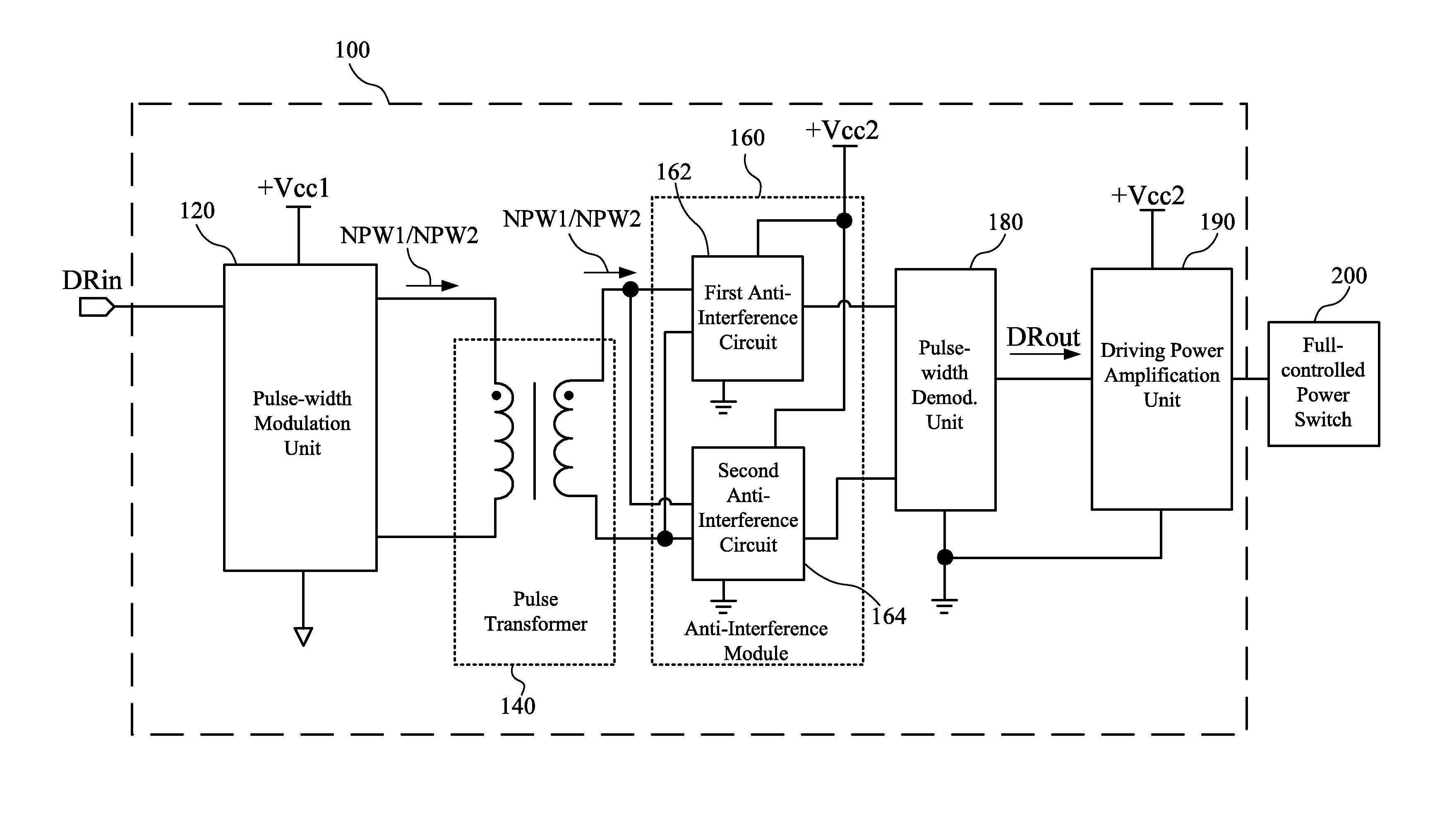
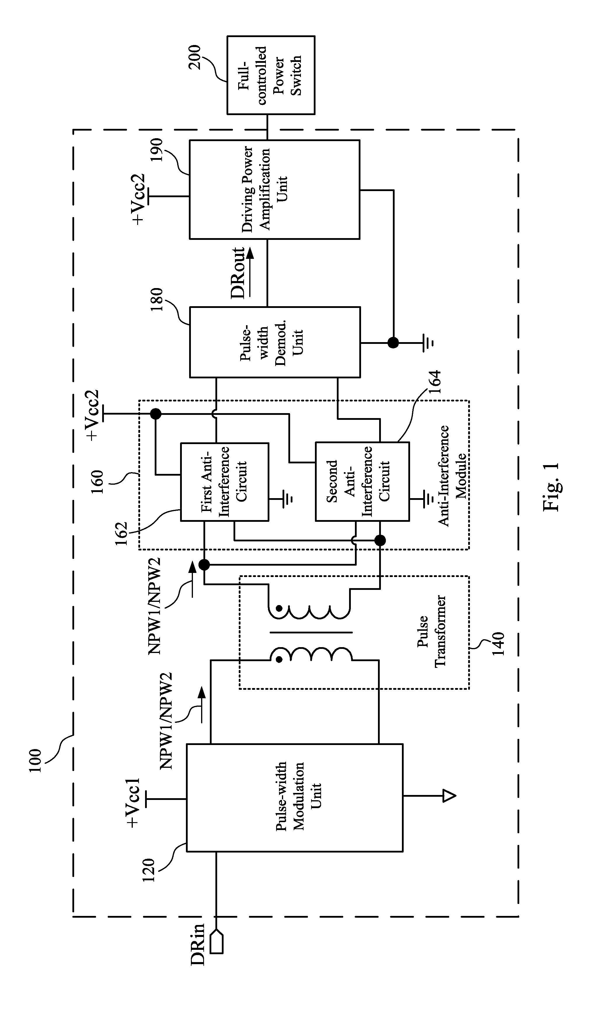
[0035]Referring to FIG. 1, it illustrates a functional block diagram of a switch driving circuit 100 according to the invention. As shown in FIG. 1, the switch driving circuit 100 includes a pulse-width modulation unit 120, a pulse transformer 140, an anti-interference module 160, a pulse-width demodulation unit 180 and a driving-power amplifier 190. The switch driving circuit 100 is coupled to a full-controlled power switch 200. The switch driving circuit 100 receives a driving input signal DRin and converts the driving input signal DRin into a driving output signal DRout. The driving output signal DRout is used for controlling the full-controlled power switch 200. In the embodiments of the invention, the full-controlled power switch 200 may include at least one set of IGBTs.

[0036]The switch driving circuit 100 magnetically isolates the driving input signal DRin from the driving output signal DRout through the pulse transformer 140 so as to avoid the mutual influence between the dr...

second embodiment

[0060]With the development of the semiconductor technology, the feature of the power device switch is improved greatly inevitably. The operation frequency of the power device switch will be very high. At this time, the frequency of the corresponding driving control signal may also be increased. When the driving control signal is an ultra-high frequency driving input signal, the pulse width of the maximum duty ratio (such as Dmax in FIG. 5) corresponding to the ultra-high frequency driving input signal is very small. The magnetic core transmission technology and the same anti-interference circuit also can transfer the ultra-high frequency signal and drive the power device, such as the switch driving circuit 300 in the

[0061]As shown in FIG. 4, according to the second embodiment of the invention, the switch driving circuit 300 includes a signal processing circuit 320, a pulse transformer 340, an anti-interference module 360 and a driving-power amplifier 390. The signal processing circu...

third embodiment

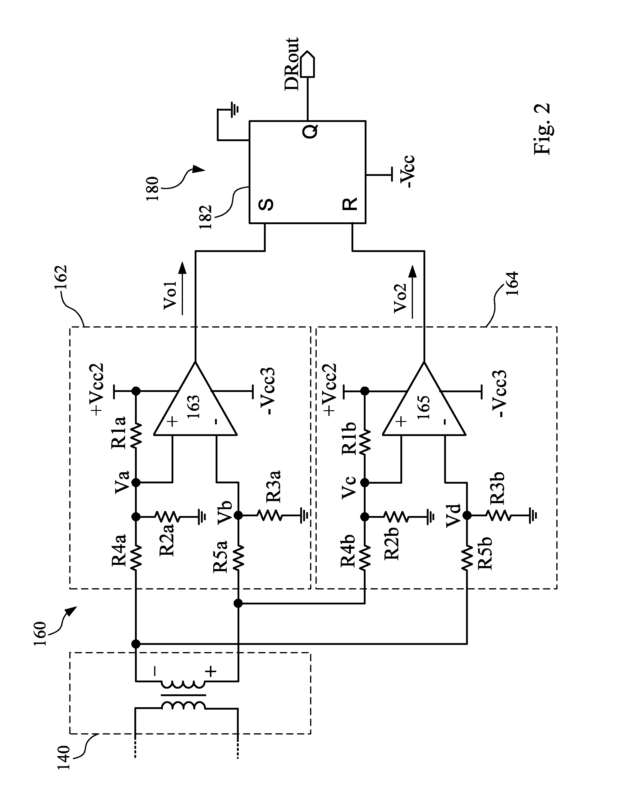
[0068]It should be supplemented that in the third embodiment the anti-interference module 560 has the impedance matching circuit 564. The impedance matching circuit 564 aims to match the impedance of the anti-interference circuit 562. Accordingly, a comparator is not necessary for the impedance matching circuit 564, and the impedance matching circuit 564 only needs to be provided with a corresponding resistor to match with the impedance of the anti-interference circuit 562, such as the first resistor R1b, the second resistor R2b (optional), the third resistor R3b, the fourth resistor R4b and the fifth resistor R5b of the impedance matching circuit 564 in FIG. 7. However, many methods can be used to realize the impedance matching and the invention is not limited to this resistor arrangement method.

[0069]In addition, the structure of the anti-interference circuit in this disclosure is not limited to the anti-interference circuit 162, 164 shown in FIG. 2 or the anti-interference circui...


PUM


Abstract

A switch driving circuit for driving a full-controlled power switch is disclosed, including a pulse-width modulation unit, a pulse transformer, an anti-interference module, a pulse-width demodulation unit and a driving-power amplifier. The pulse-width modulation unit converts a driving input signal into a positive-negative narrow pulse-width signal. The anti-interference module is coupled to the secondary side and the positive-negative narrow pulse-width signal includes multiple positive pulses and negative pulses. The anti-interference module filters out the ones from the positive pulses and negative pulses of which the pulse amplitude does not reach an effective threshold, and meanwhile the anti-interference module suppress a common-mode noise caused by a high voltage transient variation at a moment when the full-controlled power switch is turned on or off. The pulse-width demodulation unit converts the filtered positive-negative narrow pulse-width signal into a driving output signal.

Description

RELATED APPLICATIONS[0001]This application claims priority to Chinese Application Serial Number 201210298849.2, filed Aug. 21, 2012, which is herein incorporated by reference.BACKGROUND[0002]1. Field of Invention[0003]The invention relates to a switch driving circuit. More particularly, the invention relates to a switch driving circuit for driving a full-controlled power switch.[0004]2. Description of Related Art[0005]The insulated gate bipolar transistor (IGBT) is one of the full-controlled power switch elements. The input stage and the output stage of the insulated gate bipolar transistor are integrated into one device respectively through the metal-oxide-semiconductor field-effect transistor (MOSFET) and the PNP bipolar junction transistor (BJT), which has both the features of low driving power, rapid switch speed (control and response) and high input impedance of the MOSFET device and the features of reduced saturation voltage and high capacity of the bipolar device. Currently, ...

Claims


Application Information

Patent Timeline
Patent Type & Authority Applications(United States)
IPC IPC(8): H03K17/16
CPCH03K17/16H03K17/162H03K17/691
Inventor WANG, MINGFU, WEI-LIANGCONG, QINGYING, JIAN-PINGZHANG, BING
Owner DELTA ELECTRONICS INC
Why Eureka
Try Eureka