Niobium nitride and method for producing same, niobium nitride-containing film and method for producing same, semiconductor, semiconductor device, photocatalyst, hydrogen generation device, and energy system

a technology of niobium nitride and niobium nitride, which is applied in the direction of catalyst activation/preparation, metal/metal-hydroxide catalyst, catalyst activation/preparation, etc., can solve the problems of low hydrogen generation efficiency, low utilization efficiency of sunlight, and only about 6% utilization efficiency, and achieve high water stability

Active Publication Date: 2014-02-27
PANASONIC INTELLECTUAL PROPERTY MANAGEMENT CO LTD
View PDF0 Cites 149 Cited by
  • Summary
  • Abstract
  • Description
  • Claims
  • Application Information

AI Technical Summary

Benefits of technology

[0013]The niobium nitride of the present invention is a novel substance, and can be used as a semiconductor material capable of absorbing longer wavelength light (having a smaller band gap), having band edges at levels between which the oxidation-reduction potential of water is present, and having high stability in water under light irradiation.

Problems solved by technology

These conventional semiconductor electrodes have a problem of low hydrogen generation efficiency in water decomposition reaction by sunlight irradiation.
Furthermore, in view of a theoretical loss of the absorbed light due to heat loss, the sunlight utilization efficiency is only about 1.7%.
Furthermore, in view of a theoretical heat loss, the utilization efficiency is only about 6%.

Method used


Image

  • Niobium nitride and method for producing same, niobium nitride-containing film and method for producing same, semiconductor, semiconductor device, photocatalyst, hydrogen generation device, and energy system
  • Niobium nitride and method for producing same, niobium nitride-containing film and method for producing same, semiconductor, semiconductor device, photocatalyst, hydrogen generation device, and energy system
  • Niobium nitride and method for producing same, niobium nitride-containing film and method for producing same, semiconductor, semiconductor device, photocatalyst, hydrogen generation device, and energy system

Examples


first embodiment

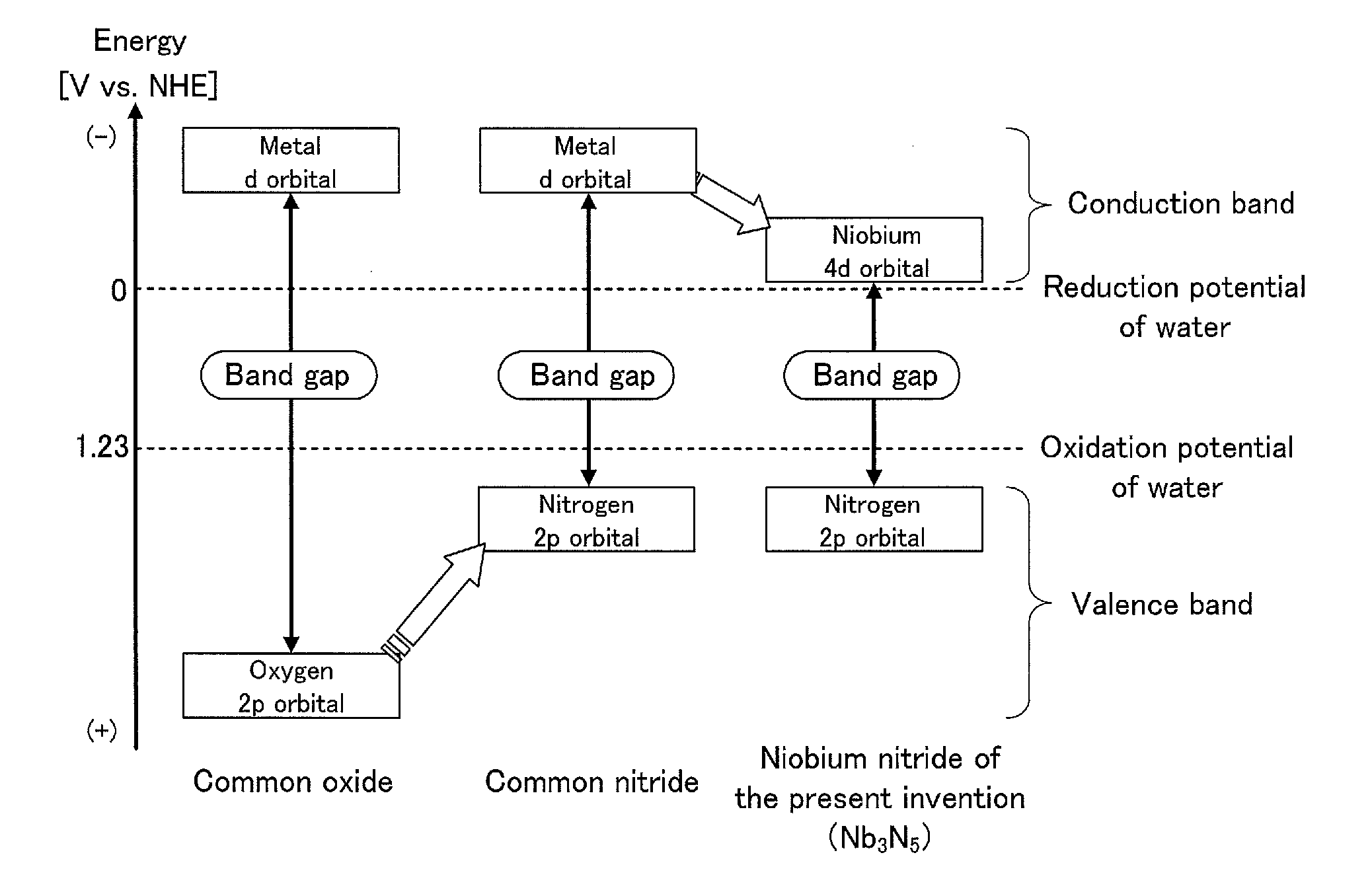
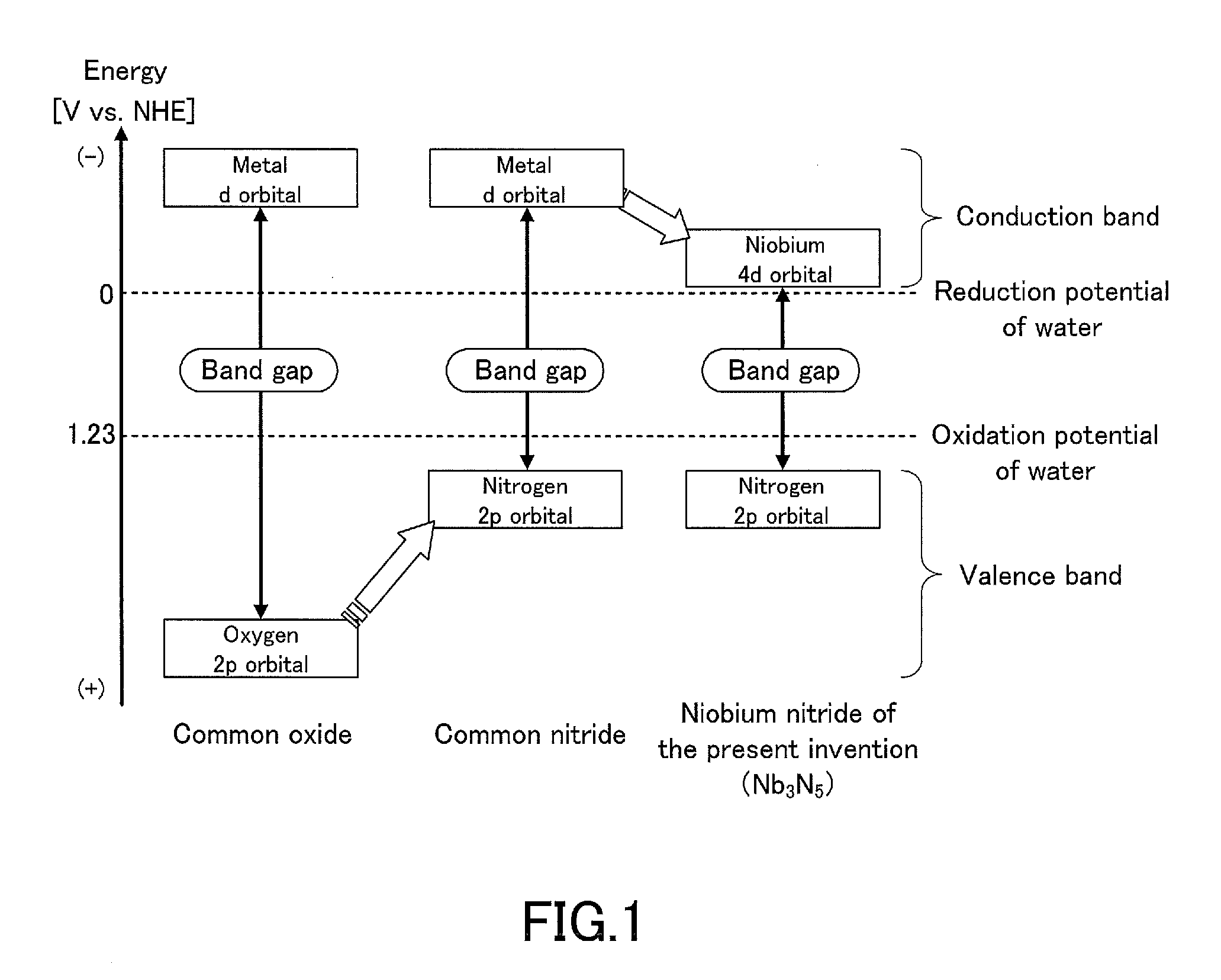
[0070]A niobium nitride according to a first embodiment of the present invention has a composition represented by the composition formula Nb3N5, and a constituent element Nb has a valence of substantially +5. This niobium nitride is synthesized by the following method.

[0071]The niobium nitride of the present embodiment can be synthesized by a method including the nitriding step of nitriding an organic niobium compound by reacting the organic niobium compound with a nitrogen compound gas.

[0072]As the organic niobium compound, a compound having a composition represented by the composition formula Nb(NR2)5, where R is an alkyl group having 1 to 3 carbon atoms, preferably 1 to 2 carbon atoms, is suitably used. Among such compounds, pentakis(dimethylamino)niobium (Nb(N(CH3)2)5) is particularly preferred. Preferably, the organic niobium compound as the starting material contains Nb(NR2)5, and more preferably it consists of Nb(NR2)5.

[0073]As the nitrogen compound gas, for example, ammonia,...

second embodiment

[0080]Another embodiment of the production method of the niobium nitride Nb3N5 of the present invention is described below.

[0081]The production method of the present embodiment includes the step of heating an organic niobium compound containing a compound represented by the composition formula R1N═Nb(NR2R3)3, where R1, R2 and R3 are each independently a hydrocarbon group, in an atmosphere containing ammonia. This step can be carried out using, for example, the apparatus 100 as shown in FIG. 3, as in the first embodiment. Preferably, the organic niobium compound as the starting material contains R1N═Nb(NR2R3)3, and more preferably it consists of R1N═Nb(NR2R3)3. Here, the case where the organic niobium compound consists of R1N═Nb(NR2R3)3 is described as an example.

[0082]In the present embodiment, Nb3N5 (Nb3N5 powder) can be synthesized by heating a raw material (R1N═Nb(NR2R3)3) 101 set in the boat 113 in the tube 112, in the gas flow 102 containing ammonia flowing through the tube 112...

third embodiment

[0089]An embodiment of the production method of the niobium nitride (Nb3N5)-containing film of the present invention is described below.

[0090]The production method of the present embodiment includes the steps of (I) vaporizing an organic niobium compound (for example Nb(NR2)5, where R is an alkyl group having 1 to 3 carbon atoms (preferably 1 to 2 carbon atoms); and (II) bringing the vaporized organic niobium compound and a nitrogen compound gas into contact with a heated substrate. These steps can be carried out using, for example, a MOCVD (Metal-Organic Chemical Vapor Deposition) apparatus 500 as shown in FIG. 5. This method makes it possible to produce a Nb3N5-containing film while suppressing the generation of NbN. In addition, this method makes it possible to produce a Nb3N5-containing film fixed to a substrate by chemical bonding. The Nb3N5-containing film obtained by the method of the present embodiment allows Nb3N5 to exhibit its excellent optical semiconductor properties be...


PUM

PropertyMeasurementUnit
wavelengthaaaaaaaaaa

Abstract

The present invention is a niobium nitride which has a composition represented by the composition formula Nb3N5 and in which a constituent element Nb has a valence of substantially +5. The method for producing the niobium nitride of the present invention includes the step of nitriding an organic niobium compound by reacting the organic niobium compound with a nitrogen compound gas.

Description

TECHNICAL FIELD[0001]The present invention relates to a niobium nitride and a method for producing the niobium nitride, a niobium nitride-containing film and a method for producing the niobium nitride-containing film, a semiconductor, a semiconductor device, a photocatalyst suitable for water decomposition reaction, a hydrogen generation device including the photocatalyst, and an energy system including the hydrogen generation device.BACKGROUND ART[0002]Conventionally, water is decomposed into hydrogen and oxygen by irradiating a semiconductor material serving as a photocatalyst with light.[0003]For example, Patent Literature 1 discloses a method in which an n-type semiconductor electrode and a counter electrode are disposed in an electrolytic solution and the surface of the n-type semiconductor electrode is irradiated with light to obtain hydrogen and oxygen from the surfaces of these electrodes. Patent Literature 1 describes the use of a TiO2 electrode, a ZnO electrode, or the lik...

Claims


Application Information

Patent Timeline
Patent Type & Authority Applications(United States)
IPC IPC(8): B01J19/12B01J27/24
CPCC04B2235/80C04B2235/79C04B35/58007C01P2002/84C01B3/042C01B21/0617C01B21/06C04B2235/465H01M8/06C01P2002/85C25B1/003B01J35/02C04B35/6325C01P2002/88Y02E60/364C04B2235/3886B01J27/24B01J19/123C04B35/62886C04B2235/3251C04B35/62805B01J23/20B01J23/6484B01J35/002B01J35/004B01J37/086H01M8/04216H01M8/0656C25B1/55Y02E60/36Y02E60/50
Inventor SUZUKI, TAKAHIRONOMURA, TAKAIKIKUROHA, TOMOHIROMIYATA, NOBUHIROTAMURA, SATORUTOKUHIRO, KENICHIHATO, KAZUHITO
Owner PANASONIC INTELLECTUAL PROPERTY MANAGEMENT CO LTD
Why Eureka
Try Eureka