System and Method for Ex Situ Analysis of a Substrate

a substrate and ex situ analysis technology, applied in liquid/fluent solid measurement, instruments, machines/engines, etc., can solve the problems of inability to accurately detect the structure of the substrate, the thinning of the substrate below 30 nm is difficult, and the measurement is too small for the resolution provided by an ordinary sem, etc., to achieve a high degree of confidence in the orientation of the substrate, the effect of easy identification of the orientation and fast processing of the lamella

Active Publication Date: 2014-03-27
FEI CO
View PDF12 Cites 22 Cited by
  • Summary
  • Abstract
  • Description
  • Claims
  • Application Information

AI Technical Summary

Benefits of technology

[0023]An object of the invention, therefore, is to provide an improved method for TEM sample analysis. Preferred embodiments of the present invention provide for improved methods for creating and using a lamella with easily identifiable orientation. Some preferred embodiments of the present invention provide the use of the lamella in an ex-situ process that allows for lamella sample placement on a carbon grid with a high degree of confidence regarding its orientation and overall faster processing of the lamella than current prior art in-situ processes.
[0024]Some preferred embodiments of the present invention provide methods to create lamella having an asymmetric shape, which allows for higher degree of orientation recognition and easier identification of the region of interest on the lamella. Some preferred embodiments of the present invention provide methods to properly place the lamella over a carbon grid containing holes such that the region of interest lies directly over one of the holes such that TEM imaging and chemical analysis of the sample results in little to no interference from the carbon.

Problems solved by technology

As features continue to get smaller and smaller, however, there comes a point where the features to be measured are too small for the resolution provided by an ordinary SEM.
Because a sample must be very thin for viewing with transmission electron microscopy (whether TEM or STEM), preparation of the sample can be delicate, time-consuming work.
Currently, thinning below 30 nm is difficult and not robust.
Thickness variations in the sample result in lamella bending, overmilling, or other catastrophic defects.
The disadvantage to these techniques is that they are not site-specific and often require that the starting material be sectioned into smaller and smaller pieces, thereby destroying much of the original sample.
The smaller back trench is primarily to save time, but the smaller trench also prevents the finished sample from falling over flat into larger milled trenches which may make it difficult to remove the specimen during the micromanipulation operation.
The use of traditional carbon grid 13 poses a technical problem.
But these methods are typically very time-consuming and labor intensive.
It further requires the sample to be welded or affixed to a TEM grid inside a vacuum chamber, which requires a large amount of valuable FIB time.
Even though the information that can be discovered by TEM analysis can be very valuable, the entire process of creating and measuring TEM samples has historically been so labor intensive and time consuming that it has not been practical to use this type of analysis for manufacturing process control.
Although ex-situ methods do not require the labor intensive and time consuming manipulation inside the vacuum chamber, they are unreliable and require a great deal of operator experience.
It can be time consuming and difficult to locate a lamella site and the extraction probe must be very carefully moved into position to avoid damaging the sample or the probe tip.
Once a lamella has been completely freed, it can move in unpredictable ways; it can fall over in the trench or in some cases it can actually be pushed up and out of the trench by electrostatic forces.
This movement can make it difficult to locate and / or pick up the lamella with the extraction probe.
The electrostatic attraction between the probe and the sample is also somewhat unpredictable.
If the lamella is successfully transferred to the TEM grid, it can be difficult to get the lamella to adhere to the grid support film rather than the probe tip.
As a result, it is difficult to control the precise placement or orientation of the lamella when it is transferred to the TEM grid.
Unfortunately, the region of interest in the lamella often exceed 2 μm in length, and the typical carbon grids with holes are not able to fully contain the region of interest.
Even with superior TEM systems, the optical chain and mechanical motion control has at least 1 μm of error during placement.
This results in a failure to properly place the region of interest in nearly 80% of the cases.
In addition, the ability to set the sample into a very specific region of interest has a large amount of uncertainty.

Method used


Image

  • System and Method for Ex Situ Analysis of a Substrate
  • System and Method for Ex Situ Analysis of a Substrate
  • System and Method for Ex Situ Analysis of a Substrate

Examples


Embodiment Construction

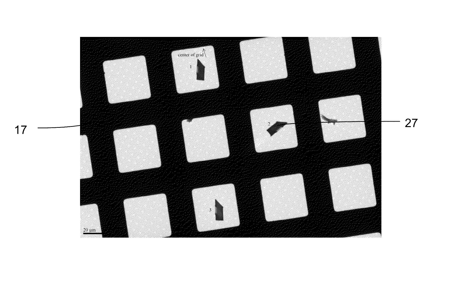
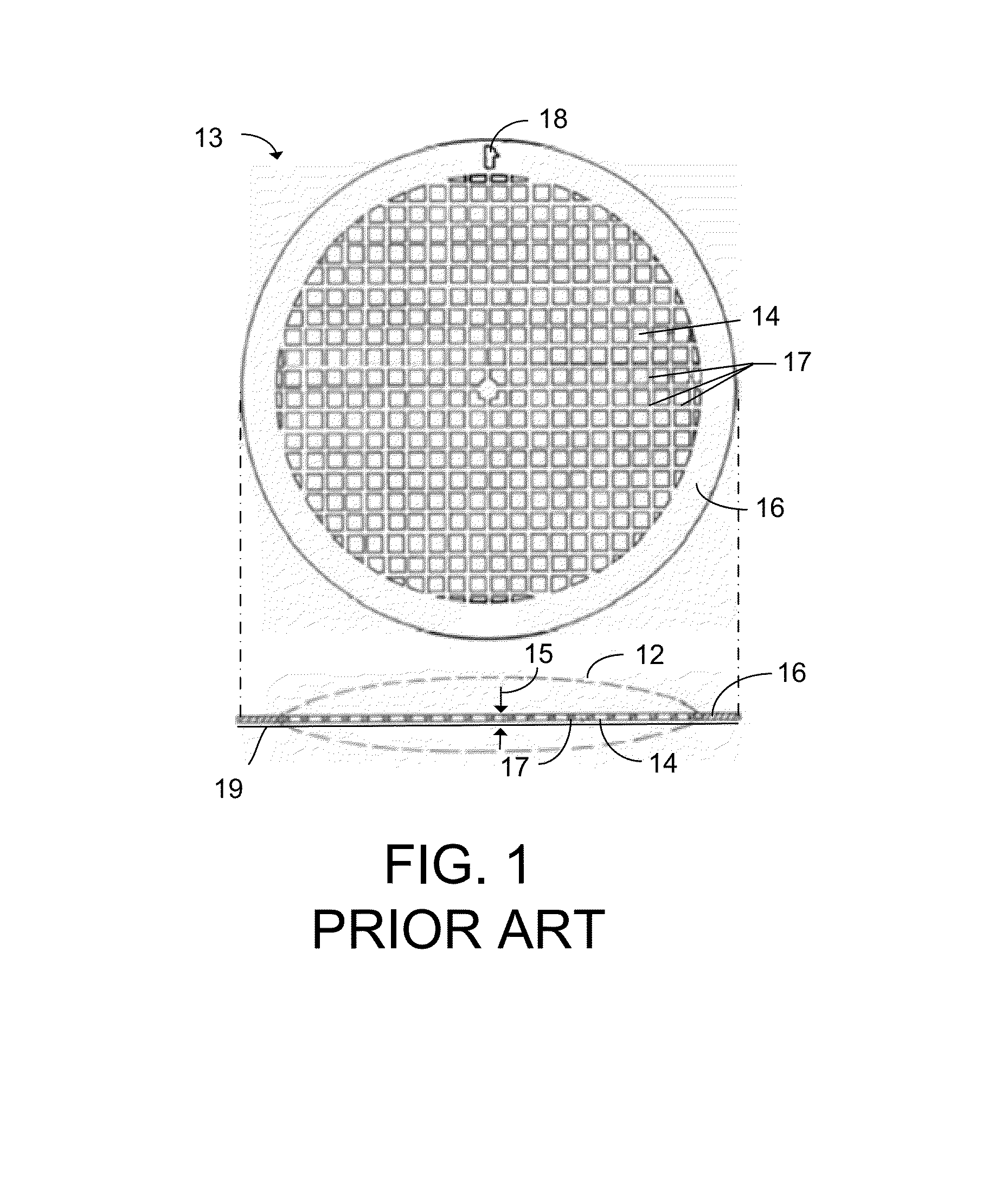
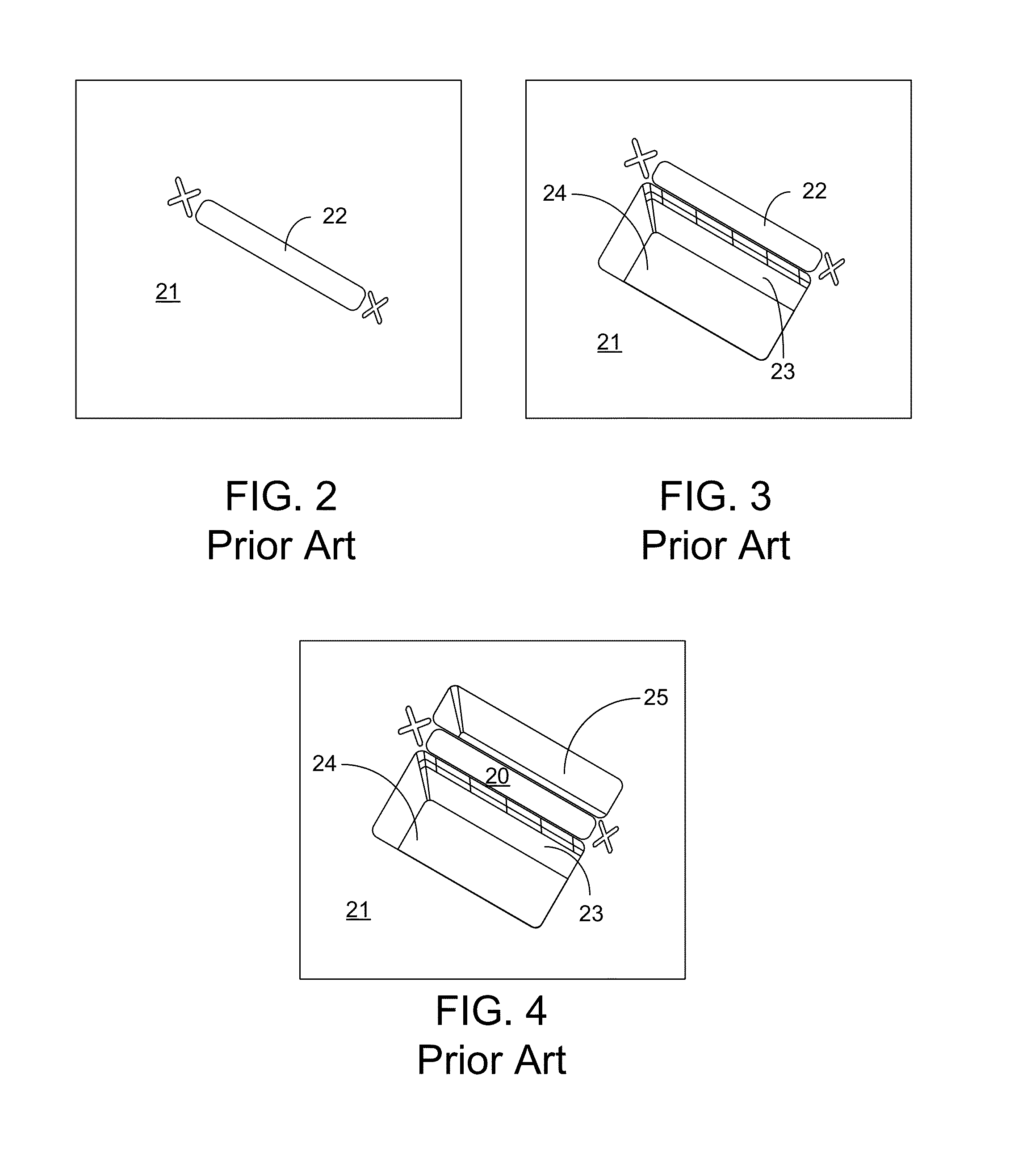
[0043]Preferred embodiments of the present invention provide for improved methods for lamella creation from wafers and use of the lamella in ex-situ processes. More specifically, preferred embodiments make lamellas in asymmetric shapes before they are extracted and placed on specified carbon grids containing a carbon film with sizeable holes. S / TEM samples produced according to the present invention will allow S / TEM imaging and chemical analysis with a high degree of confidence in sample orientation. Such orientation and methods of using ex-situ processes allow for proper placement of the sample on precise locations of the carbon grid such that the region of interest lies over one of the many sizable holes in the carbon film, which results in little to no optical and spectral interference from the carbon. Overall, the lower potential for error from knowing the orientation of the sample in combination with the faster processing of the samples in ex-situ processes and less interferenc...


PUM

PropertyMeasurementUnit
lengthaaaaaaaaaa
thicknessaaaaaaaaaa
widthaaaaaaaaaa

Abstract

A method and system for creating an asymmetrical lamella for use in an ex situ TEM, SEM, or STEM procedure is disclosed. The shape of the lamella provides for easy orientation such that a region of interest in the lamella can be placed over a hole in a carbon film providing minimal optical and spectral interference from the carbon film during TEM, SEM, or STEM procedure of chemical analysis.

Description

TECHNICAL FIELD OF THE INVENTION[0001]The present invention relates to preparation of samples and methods of sample handling for analysis by electron microscopes.BACKGROUND OF THE INVENTION[0002]Semiconductor manufacturing, such as the fabrication of integrated circuits, typically entails the use of photolithography. A semiconductor substrate on which circuits are being formed, usually a silicon wafer, is coated with a material, such as a photoresist, that changes solubility when exposed to radiation. A lithography tool, such as a mask or reticle, positioned between the radiation source and the semiconductor substrate casts a shadow to control which areas of the substrate are exposed to the radiation. After the exposure, the photoresist is removed from either the exposed or the unexposed areas, leaving a patterned layer of photoresist on the wafer that protects parts of the wafer during a subsequent etching or diffusion process.[0003]The photolithography process allows multiple inte...

Claims


Application Information

Patent Timeline
Patent Type & Authority Applications(United States)
IPC IPC(8): G01N1/28H01J37/02
CPCH01J37/02G01N1/28H01J37/3023H01J2237/31745G01N1/32H01J37/20H01J37/3056
Inventor MILLER, THOMAS G.ARJAVAC, JASONHEER, DAMONSTRAUSS, MICHAELVAN VEEN, GERARDUS NICOLAAS ANNE
Owner FEI CO
Why Eureka
Try Eureka