Self-aligned structures and methods for asymmetric GAN transistors & enhancement mode operation

a technology of gan transistors and self-aligning structures, applied in the field of microelectronic devices, can solve the problems of elusive soc solutions, limited scaling to smaller and more power efficient form factors, and inability to achieve more extensive soc solutions for mobile computing platforms

Active Publication Date: 2014-04-03
INTEL CORP
View PDF2 Cites 108 Cited by
  • Summary
  • Abstract
  • Description
  • Claims
  • Application Information

AI Technical Summary

Problems solved by technology

Because current platform solutions for smart phones and tablets rely on multiple packaged integrated circuits (ICs) mounted onto a circuit board, further scaling to smaller and more power efficient form factors is limited.
While the logic processor IC may itself be considered a system on a chip (SoC) integrating both memory and logic functions, more extensive SoC solutions for mobile computing platforms have remained elusive because the PMIC and RFIC operate with two or more of high voltage, high power, and high frequency.
While an SoC solution for the mobile computing space that would integrate PMIC and RFIC functions is attractive for improving scalability, lowering costs, and improving platform power efficiency, one barrier to such an SoC solution is the lack of a scalable transistor technology having both sufficient speed (i.e., sufficiently high gain cutoff frequency, Ft), and sufficiently high breakdown voltage (BV).
To date, no technique exists to repeatedly define these device dimensions to different values.
Conventional methods rely on alignment of two or more lithographic mask patterning operations and such techniques suffer from high variation of Lgd and Lsg dimensions due to inter-mask alignment tolerances / errors.
Enhancement mode operation also remains a challenge for III-N HEMT devices with thresholds in most designs being less than zero (i.e., depletion mode).
Large scale integration of III-N HEMTs thus poses power consumption concerns.
Conventional threshold adjustment techniques typically rely on gate recess etches (e.g., single or double recess), but limited etch selectivity may make such techniques unsuitable for high volume manufacturing.

Method used


Image

  • Self-aligned structures and methods for asymmetric GAN transistors & enhancement mode operation
  • Self-aligned structures and methods for asymmetric GAN transistors & enhancement mode operation
  • Self-aligned structures and methods for asymmetric GAN transistors & enhancement mode operation

Examples


Embodiment Construction

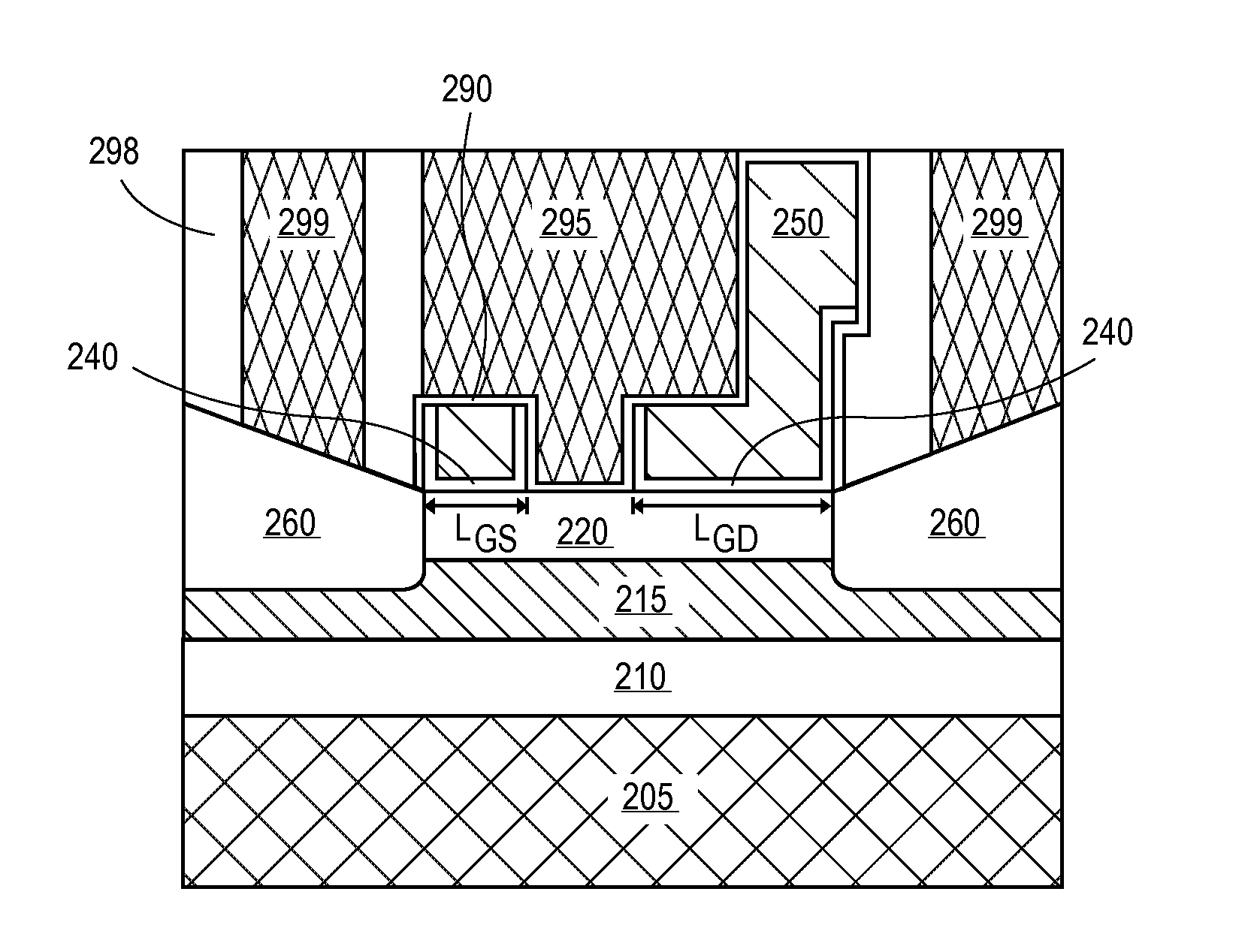
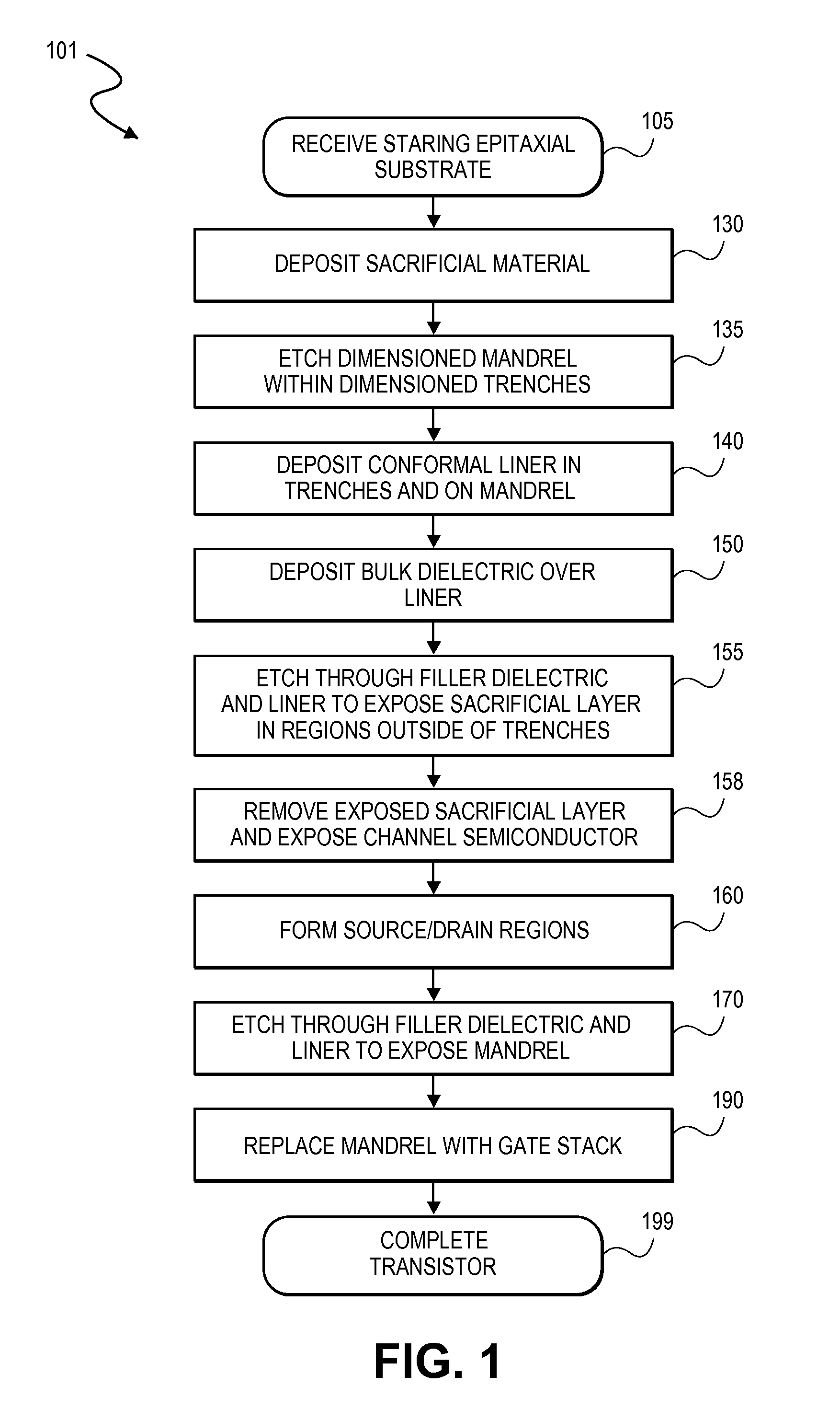
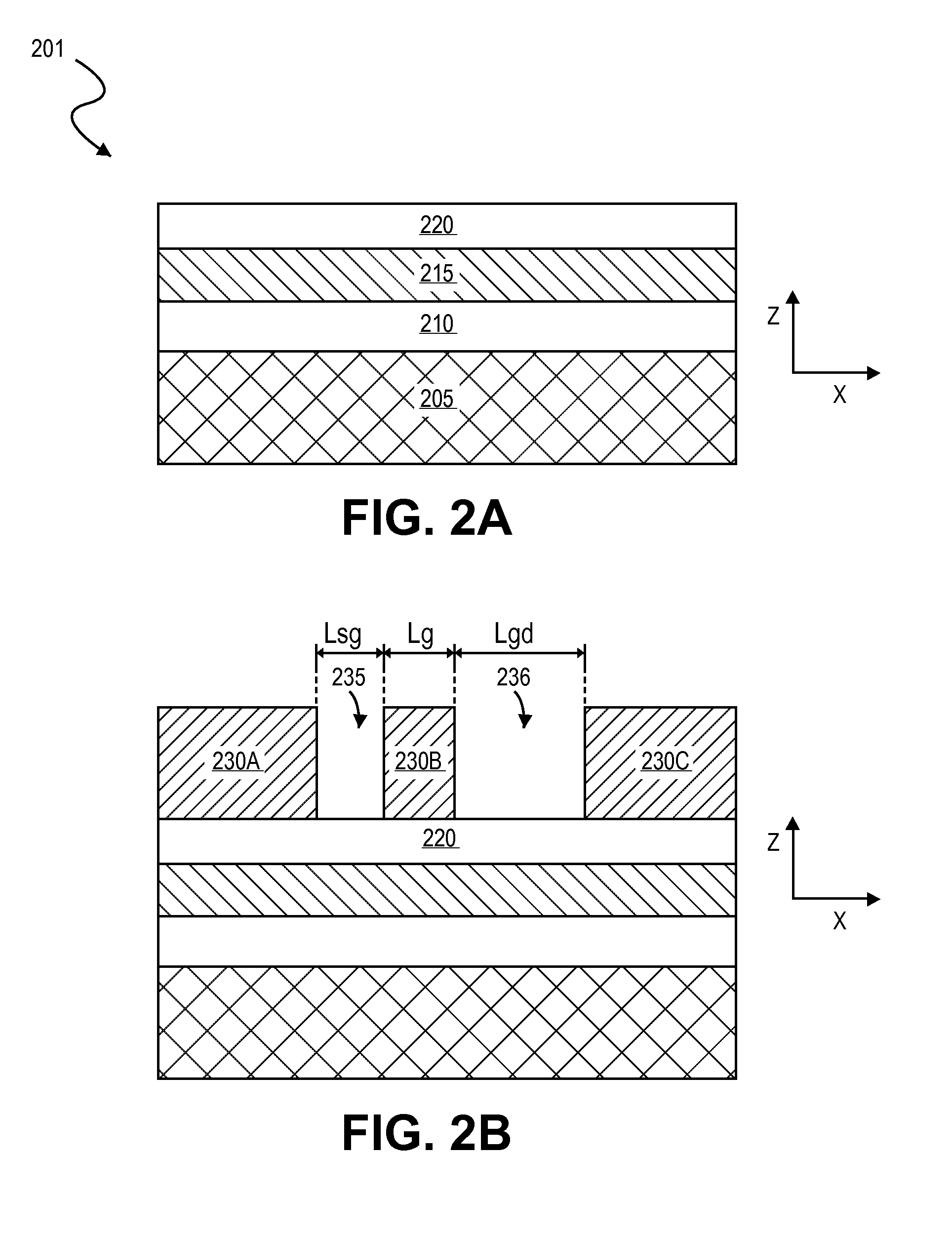
[0011]In the following description, numerous details are set forth, however, it will be apparent to one skilled in the art, that the present invention may be practiced without these specific details. In some instances, well-known methods and devices are shown in block diagram form, rather than in detail, to avoid obscuring the present invention. Reference throughout this specification to “an embodiment” means that a particular feature, structure, function, or characteristic described in connection with the embodiment is included in at least one embodiment of the invention. Thus, the appearances of the phrase “in an embodiment” in various places throughout this specification are not necessarily referring to the same embodiment of the invention. Furthermore, the particular features, structures, functions, or characteristics may be combined in any suitable manner in one or more embodiments. For example, a first embodiment may be combined with a second embodiment anywhere the two embodi...


PUM


Abstract

Embodiments include high electron mobility transistors (HEMT). In embodiments, a gate electrode is spaced apart by different distances from a source and drain semiconductor region to provide high breakdown voltage and low on-state resistance. In embodiments, self-alignment techniques are applied to form a dielectric liner in trenches and over an intervening mandrel to independently define a gate length, gate-source length, and gate-drain length with a single masking operation. In embodiments, III-N HEMTs include fluorine doped semiconductor barrier layers for threshold voltage tuning and/or enhancement mode operation.

Description

TECHNICAL FIELD[0001]Embodiments of the present invention generally relate to microelectronic devices, and more particularly to group III-N transistor architecture and fabrication.BACKGROUND[0002]The mobile computing (e.g., smart phone and tablet) markets benefit from smaller component form factors and lower power consumption. Because current platform solutions for smart phones and tablets rely on multiple packaged integrated circuits (ICs) mounted onto a circuit board, further scaling to smaller and more power efficient form factors is limited. For example, a smart phone will include a separate power management IC (PMIC), radio frequency IC (RFIC), and WiFi / Bluetooth / GPS IC, in addition to a separate logic processor IC. System on Chip (SoC) architectures offer the advantage of scaling which cannot be matched by board-level component integration. While the logic processor IC may itself be considered a system on a chip (SoC) integrating both memory and logic functions, more extensive...

Claims


Application Information

Patent Timeline
Patent Type & Authority Applications(United States)
IPC IPC(8): H01L29/778H01L21/335
CPCH01L29/66462H01L29/7787H01L29/42376H01L29/0847H01L29/2003H01L29/7786H01L29/207H01L21/2654H01L21/2236H01L21/2233H01L29/205H01L21/31111H01L21/0254H01L21/31144H01L21/26546H01L29/7784
Inventor DASGUPTA, SANSAPTAKTHEN, HAN WUIRADOSAVLJEVIC, MARKOMUKHERJEE, NILOYGOEL, NITIKABEHIE, SANAZSUNG, SEUNG HOONPILLARISETTY, RAVICHAU, ROBERT S.
Owner INTEL CORP
Why Eureka
Try Eureka