Photoelectric conversion element and photoelectric conversion element module
a technology of photoelectric conversion element and conversion element, which is applied in the direction of electrolytic capacitors, light-sensitive devices, power plants, etc., can solve the problems of high production cost of thin-film solar cells, high production cost of silicon substrate cells, and foregoing problems have not yet been solved, so as to improve the light-scattering effect of reflective layers and high photoelectric conversion efficiency
- Summary
- Abstract
- Description
- Claims
- Application Information
AI Technical Summary
Benefits of technology
Problems solved by technology
Method used
Image


Examples
example 1
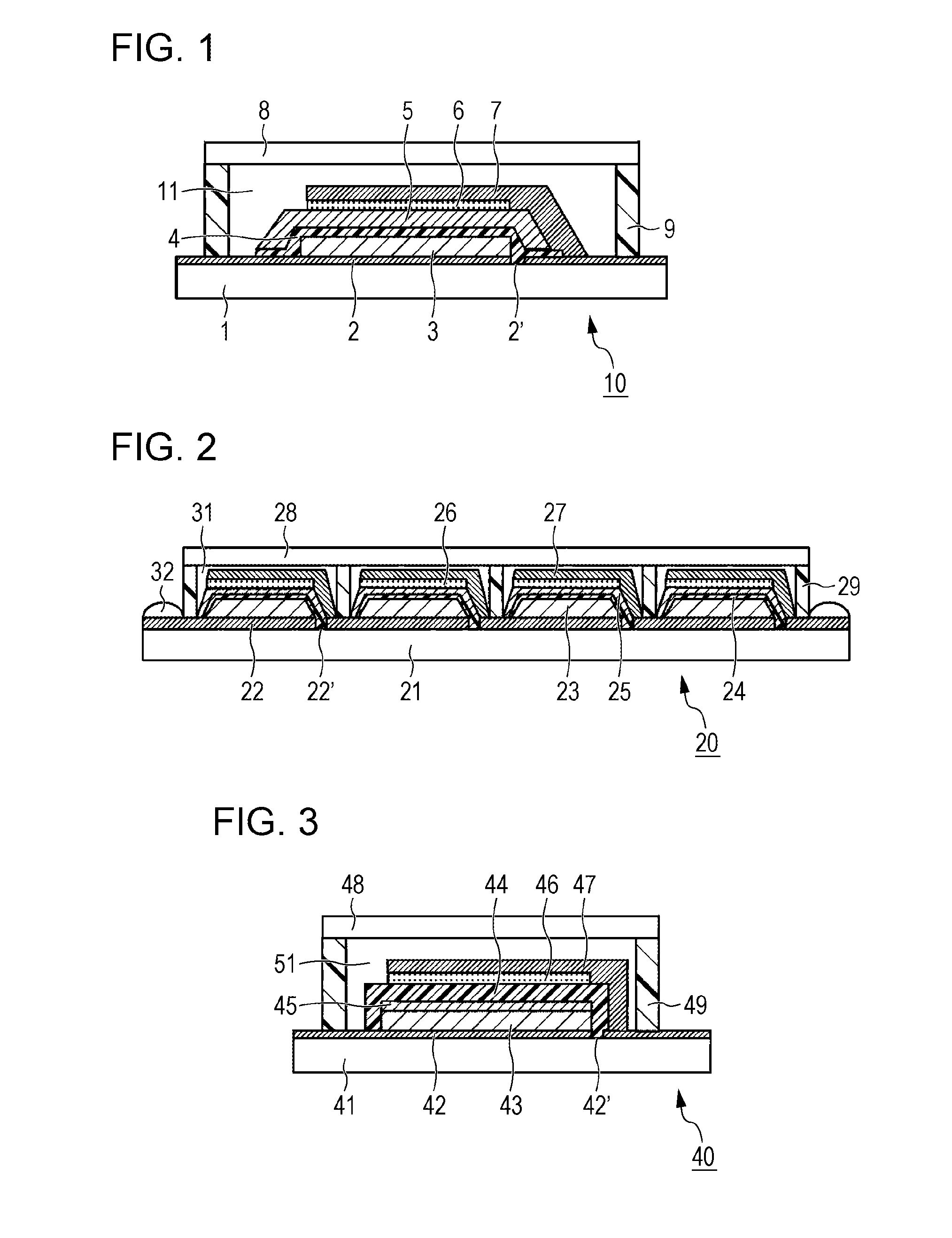
[0096]In this example, the photoelectric conversion element 10 illustrated in FIG. 1 was produced. A 15 mm×40 mm×1.5 mm thick transparent electrode substrate (glass with a SnO2 film, manufactured by Nippon Sheet Glass Company, Ltd) was prepared. The transparent electrode substrate includes the transparent conductive layer 2 composed of fluorine-doped SnO2 on the transparent substrate 1 composed of glass.
[0097]The transparent conductive layer 2 on the transparent electrode substrate was cut by laser scribing to form the scribe line 2′. A commercially available titanium oxide paste (trade name: D / SP, manufactured by Solaronix) was applied onto the transparent conductive layer 2 with a screen printing machine (Model: LS-150, manufactured by Newlong Seimitsu Kogyo Co., Ltd.) using a screen plate having a 5 mm×30 mm pattern. Leveling was performed at room temperature for 1 hour.
[0098]The resulting coating film of the titanium oxide paste was dried in an oven set at 80° C. for 20 minutes....
examples 2 to 4
[0107]Photoelectric conversion elements of Examples 2 to 4 were produced as in Example 1, except that the thicknesses of the porous insulating layers were different from those in Example 1 as described in Table 1.
example 5
[0108]A photoelectric conversion element of Example 5 was produced as in Example 1, except that the material of the porous insulating layer was changed to silicon oxide.
PUM
 Abstract
Description
Claims
Application Information