Plasma Etch Resistant Films, Articles Bearing Plasma Etch Resistant Films and Related Methods

a technology of plasma etching and resistant films, applied in the field of plasma etching resistant films, articles bearing plasma etching resistant films and related methods, can solve the problems of increasing production costs, affecting the production efficiency of plasma etching, so as to increase the plasma etching resistance of a substrate and increase the fracture toughness

Inactive Publication Date: 2014-04-10
GREENE TWEED TECH
View PDF0 Cites 37 Cited by
  • Summary
  • Abstract
  • Description
  • Claims
  • Application Information

AI Technical Summary

Benefits of technology

[0010]Several methods are contemplated within the scope of the invention. A method of manufacturing an article comprising depositing an yttria material on a substrate to form a film, wherein the film comprises the yttria material and at least a portion of the yttria material present in the film is in a crystal phase having a crystal lattice structure, wherein at least 50% of the yttria material present in the film is in a form of a monoclinic crystal system. Also included is a method of increasing the plasma etch resistance of a substrate comprising depositing a yttria material on the substrate to form a film on the surface(s) of the substrate, wherein the film comprises the yttria material and at le...

Problems solved by technology

These materials, however, may be easily eroded during routine processing conditions whether chemically, physically, and/or thermally.
Although these films often exhibit improved plasma resistance in the form of reduced weight loss, they still frequently generate unwanted particulates.
Particulates liberated in the processing chamber resul...

Method used


Image

  • Plasma Etch Resistant Films, Articles Bearing Plasma Etch Resistant Films and Related Methods
  • Plasma Etch Resistant Films, Articles Bearing Plasma Etch Resistant Films and Related Methods
  • Plasma Etch Resistant Films, Articles Bearing Plasma Etch Resistant Films and Related Methods

Examples


example i

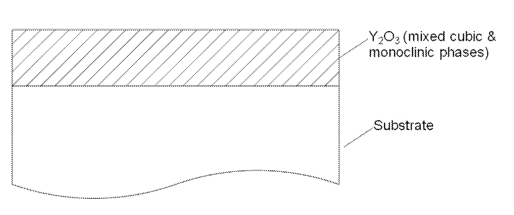
[0041]Two sets of yttrium oxide films were grown on fused quartz coupons (dimensions: 1 inch×1 inch; ⅛ inch thick) through reactive deposition using electron beam evaporation. Each coupon was installed in the electron beam film chamber and the chamber was placed under vacuum overnight. The film chamber vacuum level was maintained at 5×10⁻⁶ torr (or lower) and preheated for at least 1 hour to ensure temperature equilibrium was reached.

[0042]High purity (>99.9%) yttrium metal target was evaporated by electron beam and oxygen was bled in to the chamber to maintain a chamber process pressure between 5.5×10⁻⁵ torr to 1×10⁻⁴ torr. Each coupon was coated for 4 hours to reach target thickness of about 4 microns. During the film process, temperature of the substrate was maintained between about 250° C. to about 350° C.

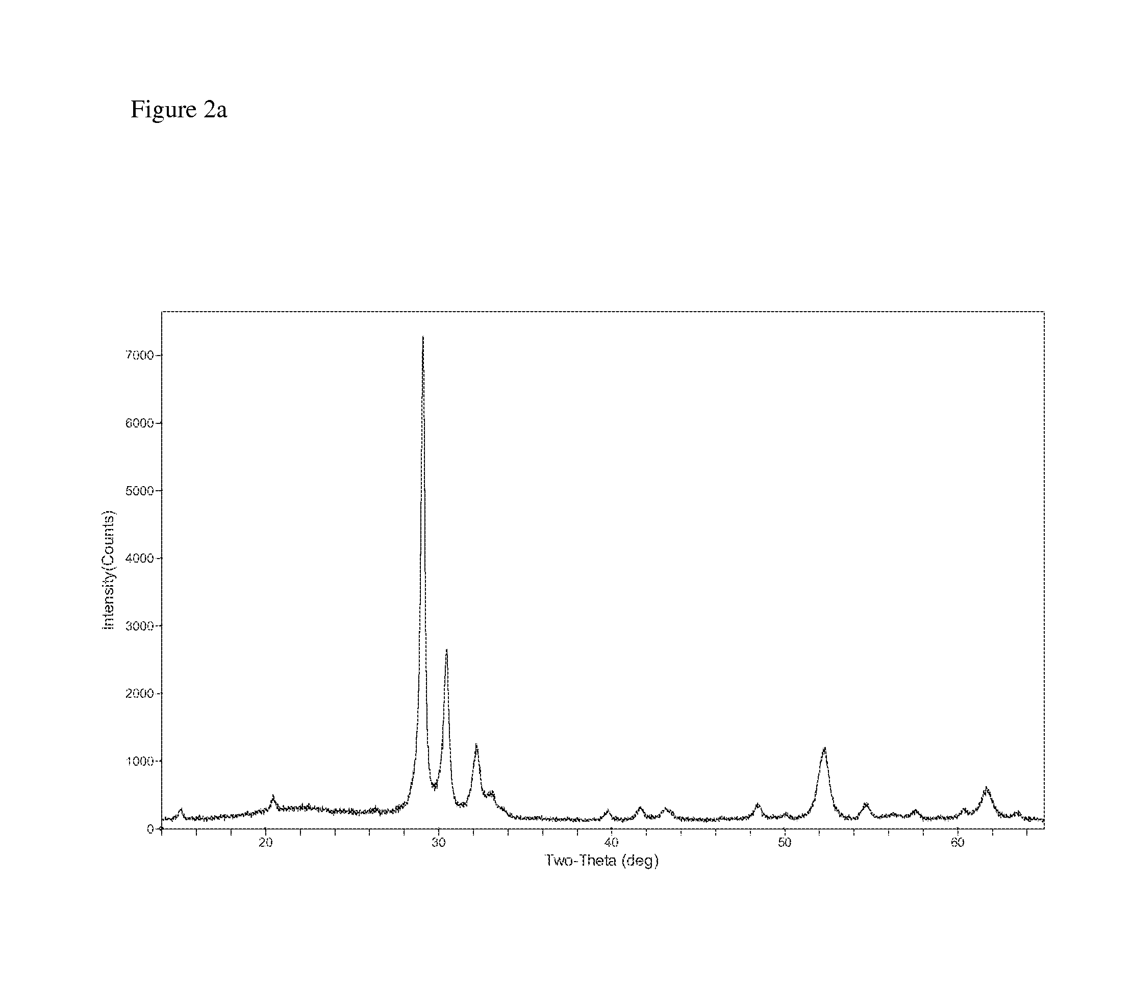
[0043]One set of films was grown to produce an yttria film containing approximately 50% cubic phase and 50% monoclinic phase. The second set was grown to produce films containi...

example 2

[0048]Three sets of yttria films on quartz coupons were prepared using standard deposition conditions. One set of films was processed further by exposing the films to a direct NF3 plasma in a capacitively coupled parallel plate reactive ion etch (RIE) reactor. Another set was processed by exposing the films to a remote NF3 plasma source. The third set of films had no further processing after coating. The films were then thermally cycled on a hot stage equipped microscope and the point of fracture formation was recorded. Yttrium oxide films for thermal cycle experiments were grown on fused quartz coupons (dimensions: 1 inch×1 inch; ⅛ inch thick) by electron beam evaporation. Each coupon was installed in the electron beam film chamber and the chamber was placed under vacuum overnight. The film chamber vacuum level was maintained at 5×10⁻⁶ torr(or lower) and preheated for at least 1 hour to ensure temperature equilibrium was reached. High purity (>99.9%) yttrium metal target was evapor...


PUM

PropertyMeasurementUnit
Temperatureaaaaaaaaaa
Fractionaaaaaaaaaa

Abstract

The invention includes a plasma etch-resistant film for a substrate comprising a yttria material wherein at least a portion of the yttria material is in a crystal phase having a crystal lattice structure, wherein at least 50% of the yttria material is in a form of a monoclinic crystal system. The film may be treated by exposure to a fluorine gas plasma. Also included are plasma etch-resistant articles that include a substrate and a film, wherein the film comprises an yttria material and at least a portion of the yttria material is present in the film in a crystal phase having a crystal lattice structure and at least 50% of the yttria material is in a form of a monoclinic crystal system. Several methods are contemplated within the scope of the invention.

Description

CROSS REFERENCE TO RELATED APPLICATION[0001]This application claims the benefit under 35 U.S.C. §119(e) to U.S. Provisional Patent Application No. 61 / 544,022, filed Oct. 6, 2011, the entire disclosure of which is incorporated herein by reference.BACKGROUND OF THE INVENTION[0002]Resistance to plasmas is a desirable property for components used in processing chambers where corrosive environments are present. Process chambers and component apparatus present within or used in conjunction with processing chambers which are used in the fabrication of electronic devices and MEMS are frequently constructed from various substrates such as sapphire, silica, fused silica, quartz, fused quartz, alumina, silicon, aluminum, anodized aluminum, zirconium oxide, an aluminum alloy, and sapphire, as these materials are known to have a level of plasma resistance and / or are commonly used in semicon apparatuses for other reasons.[0003]These materials, however, may be easily eroded during routine processi...

Claims


Application Information

Patent Timeline
IPC IPC(8): C01F17/00C23C16/40H01L21/02C01F17/235
CPCC01F17/0043C23C16/405H01L21/02192C23C14/0021C23C14/083C01F17/235
Inventor AMEEN, MOHAMMEDLEE, SANG-HOMERCER, THOMASVORSA, VASIL
Owner GREENE TWEED TECH
Why Eureka
Try Eureka