Hybrid solar cell contact

a solar cell and hybrid technology, applied in the direction of sustainable manufacturing/processing, climate sustainability, semiconductor devices, etc., can solve the problems of inability to reliably screen-print metal lines of width less than 100 microns in large-scale commercial production, the spacing is too large to allow the use of emitters with sheet resistivity above and the general response of emitters with sheet resistivity below 100 ohms per square to short wavelength light, etc., to preven

Inactive Publication Date: 2014-04-17
NEWSOUTH INNOVATIONS PTY LTD
View PDF13 Cites 9 Cited by
  • Summary
  • Abstract
  • Description
  • Claims
  • Application Information

AI Technical Summary

Benefits of technology

[0042]Importantly, by using a screen-printed paste that does not penetrate through the dielectric layer during firing, contact between the screen-printed metal (typically silver) and the lightly doped silicon is avoided. Generally, metal screen printing pastes have special additives to allow them to eat through dielectric layers such as silicon nitride or silicon dioxide etc. Without these additives, the pastes can't penetrate through the dielectric layers used for passivation and antireflection on modern silicon solar cells. By refraining from using these additives the fired metal paste can be prevented from penetrating the dielectric.

Problems solved by technology

However the most fundamental limitation results from the inability to reliably screen-print metal lines of width less than 100 microns in large scale commercial production.
This spacing is too great to allow emitters with sheet resistivity above 100 ohms per square to be used due to excessive lateral resistance losses in the emitter.
However emitters with sheet resistivity below 100 ohms per square generally suffer from poor response to short wavelength light as the collection probabilities for charge generated within the emitter fall to well below unity.
Below 80 ohms per square, some loss in short wavelength response is inevitable.
Due to the large width of screen printed metal lines of 100 microns or more, such a close spacing is not possible without shading well over 10% of the cell surface.
However the conductivity of such semiconductor fingers is quite limited with sheet resistivities of below 2 ohms per square being difficult to achieve without thermal treatments that will cause damage to the wafer.
Such fingers are therefore limited in their length if they are not to incur excessive resistive losses.
This length limitation in turn typically limits the spacing between the screen-printed contacts to values not much greater than used in conventional screen-printed devices.
The main problems for this technology are that firstly, the conductivity of the semiconductor fingers 22 cannot be made high enough to be practical in a way that allows the screen-printed lines 17 to be spaced significantly further apart to reduce metal shading losses; secondly, the screen-printed metal lines 17 do not make good electrical contact to the lightly doped emitter 14 and the interface area between the semiconductor fingers 22 and the screen-printed metal 17 is not high enough to reliably make good electrical contact in large scale production; and thirdly, the metal / silicon interface area is not reduced unless a dielectric layer is used underneath the metal which will in turn cause a detrimental effect to the electrical contact between the metal and silicon.
For example variability in this contact resistance between the screen-printed metal and silicon is a weakness in the design causing efficiencies in pilot production of the technology to vary from 16.5% to 18.4%, with the average being well below 18%.
The low yields experienced in pilot production and failure to achieve the required level of finger conductivity are likely contributors to absence of commercial use.
Without these additives, the pastes can't penetrate through the dielectric layers used for passivation and antireflection on modern silicon solar cells.

Method used


Image

  • Hybrid solar cell contact
  • Hybrid solar cell contact
  • Hybrid solar cell contact

Examples


example 1

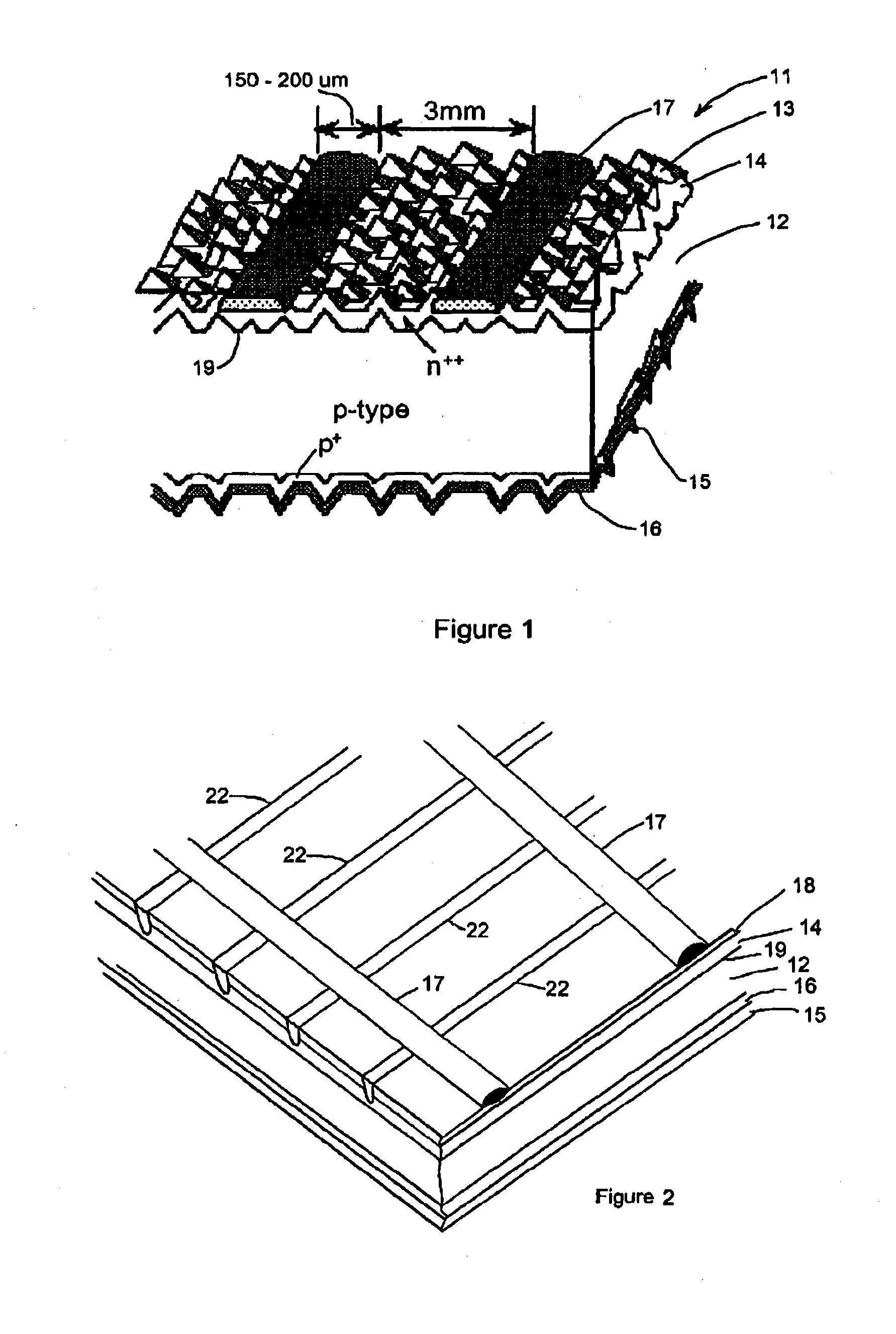
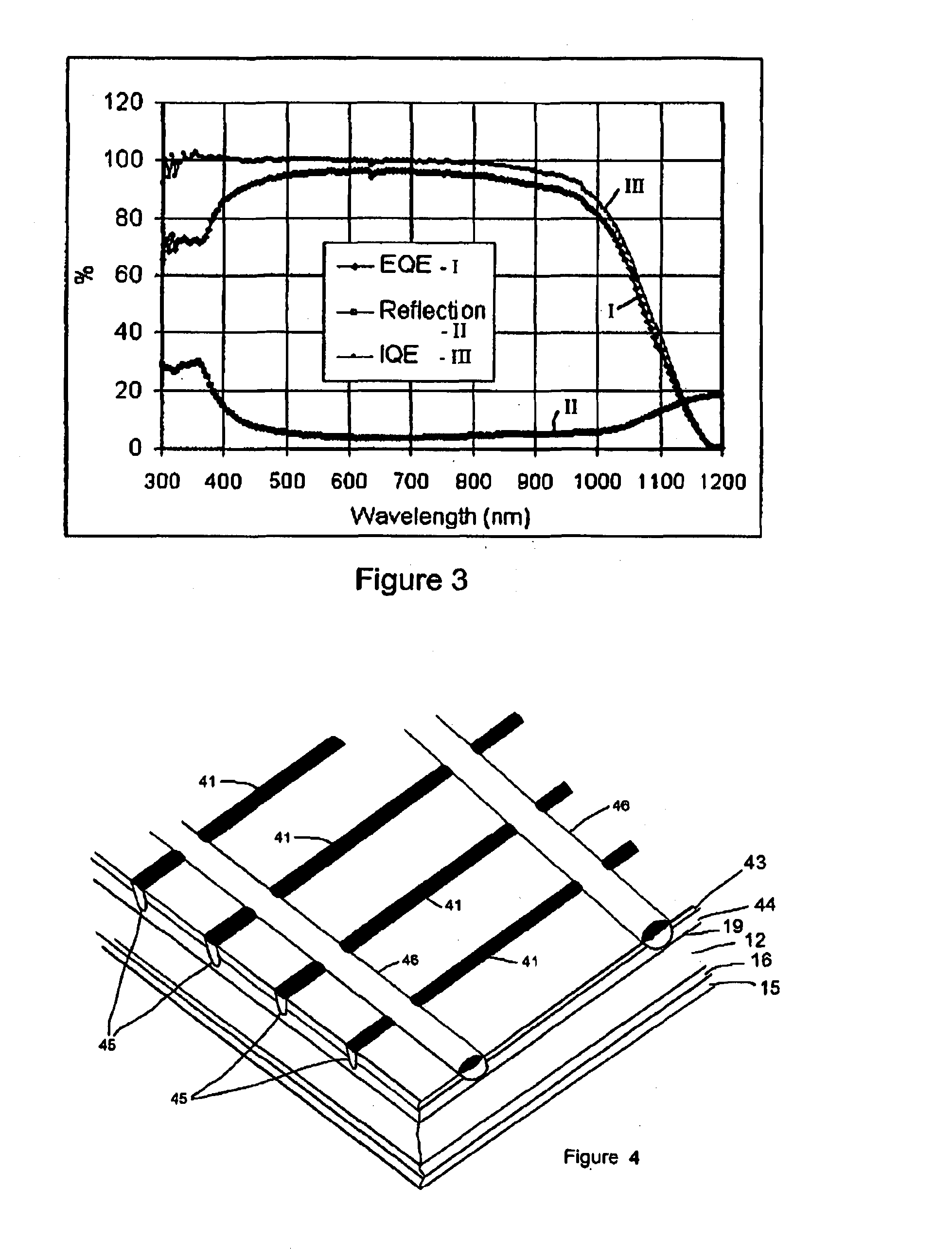
[0076]A typical processing sequence to form these hybrid contact devices is as follows:[0077]1. Surface etching and texturing of the semiconductor substrate;[0078]2. Front surface diffusion to form an emitter with sheet resistivity of at least 90 ohms / square[0079]3. PhosphoSilicate Glass removal and rear surface etch for edge junction isolation;[0080]4. PECVD deposition of top surface dielectric layer 43 such as silicon nitride or silicon oxynitride or silicon dioxide or aluminium oxide, etc;[0081]5. Screen-print front and rear metal contacts 62, 63 at a spacing of 3 to 6 mm (grid on front)[0082]6. Firing of screen-printed metal contacts at a temperature in the range of 750-850° C., simultaneously creating the rear field 16;[0083]7. Coat the surface of the dielectric layer 43 with phosphoric acid 91 as a dopant source and pattern the surface with a laser 92, while simultaneously melting the silicon to allow it to be heavily doped with phosphorus, producing narrow parallel doped line...

example 2

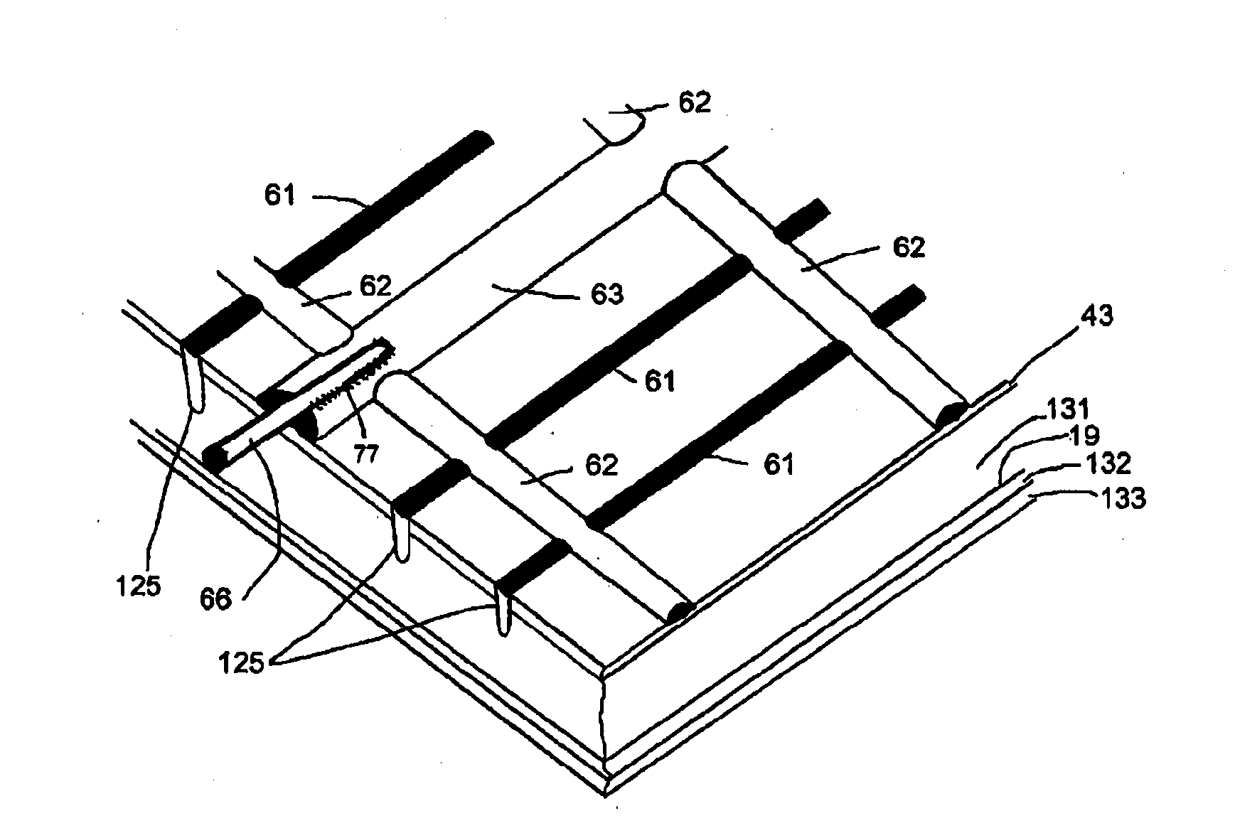
[0087]An alternative processing sequence to form these hybrid contact devices is as follows:[0088]1. Surface etching and texturing of the semiconductor substrate;[0089]2. Front surface diffusion to form an emitter 44 with sheet resistivity of at least 90 ohms / square[0090]3. PhosphoSilicate Glass removal and rear surface etch for edge junction isolation;[0091]4. PECVD deposition of surface dielectric layer 43 such as silicon nitride or silicon oxynitride or silicon dioxide or aluminium oxide, etc;[0092]5. Coat the surface of the dielectric layer 43 with phosphoric acid 91 as a dopant source and pattern the surface with a laser 92, while simultaneously melting the silicon to allow it to be heavily doped with phosphorus, producing narrow parallel doped lines 65 of exposed silicon of width 3-30 microns and spaced 0.5 to 1.5 mm apart;[0093]6. Screen-print front and rear metal contacts 62, 63 at a spacing of 3 to 6 mm whereby the silver fingers on the front are printed perpendicular or at...


PUM


Abstract

A solar cell and a method of forming a solar cell comprising: a semiconductor body having a p-n junction located between a front (light receiving) semiconductor region and a back (non-light receiving) semiconductor region; a dielectric layer extending over a front surface of the front semiconductor region; one or more elongate semiconductor fingers formed on the front surface of the front semiconductor region, the semiconductor fingers being exposed through the dielectric layer, more heavily doped than the remainder of the front semiconductor region and of the same dopant polarity; one or more elongate plated contacts formed to self align with and at least partially cover the semiconductor fingers; one or more metal collection fingers extending over the dielectric layer, generally transversely to the plated contacts.

Description

INTRODUCTION[0001]The present invention relates to solar cells and in particular to a new method of making electrical connection to such cells.BACKGROUND[0002]Screen-printed solar cells continue to dominate commercial manufacturing with well over 50% market share. The device of FIG. 1 (not to scale) shows, by way of example, a silicon solar cell 11 with screen printed contacts and includes a p-type wafer 12 with isotropic texturing 13 of the front surface (throughout this specification the term “front surface” refers to the light receiving surface and the terms “rear surface” or “back surface” refer to the non-light receiving surface), a front surface diffusion of n-type dopant 14, to form p-n junction 19, a screen-printed rear (non-light receiving) surface contact, a back surface field 16, and screen-printed front surface contacts 17. The fundamental limitations of the conventional screen-printed solar cell 11 as shown in the schematic of FIG. 1, that have limited its performance f...

Claims


Application Information

Patent Timeline
Patent Type & Authority Applications(United States)
IPC IPC(8): H01L31/0352H01L31/0224
CPCH01L31/022433H01L31/03529H01L31/022425H01L31/068H01L31/1804Y02E10/547Y02P70/50
Inventor WENHAM, STUART ROSSMAI, LY
Owner NEWSOUTH INNOVATIONS PTY LTD
Why Eureka
Try Eureka