
Silicon wafer and method for producing the same

Active Publication Date: 2014-04-17
SHIN-ETSU HANDOTAI CO LTD
View PDF5 Cites 4 Cited by
  • Summary
  • Abstract
  • Description
  • Claims
  • Application Information

AI Technical Summary

Benefits of technology

The present invention provides a method for producing a silicon wafer with reduced defects and a high yield. By heat treatment and repolishing steps, heavy metals on the surface of the wafer are removed, resulting in a reduction of micro-LPDs that cause inspection failures and device failures. The resulting silicon wafer has a low failure-incidence rate and is suitable for use in semiconductor device fabrication and production.

Problems solved by technology

It has been reported that a cause of formation of these micro LPDs is heavy-metal contamination of a wafer.
For example, typical heavy-metal contamination is contamination by copper (Cu) and occurs in a polishing step, a cleaning step, a heat treatment step, or the like by which a wafer is produced.
The copper contamination easily occurs because the rate of diffusion of copper is faster than those of other heavy metals.
However, even in a wafer produced by adequately controlling heavy-metal contamination in a wafer production step, there are still sometimes a large number of LPDs.
Moreover, in such a wafer, there are cases that the LPDs can not be reduced even when cleaning is performed after heat treatment at 600° C. or lower, the wafer is judged to be a failure in an inspection step and a shipment stage of the wafer, and yields are reduced.
Furthermore, if there is contamination by a tiny amount of heavy metal during silicon single crystal growth, as described in Patent Literature 4, LPDs continuously increase even when a wafer is cleaned after heat treatment, and it is impossible to reduce the LPDs.

Method used


Image

  • Silicon wafer and method for producing the same
  • Silicon wafer and method for producing the same
  • Silicon wafer and method for producing the same

Examples


experimental example 1

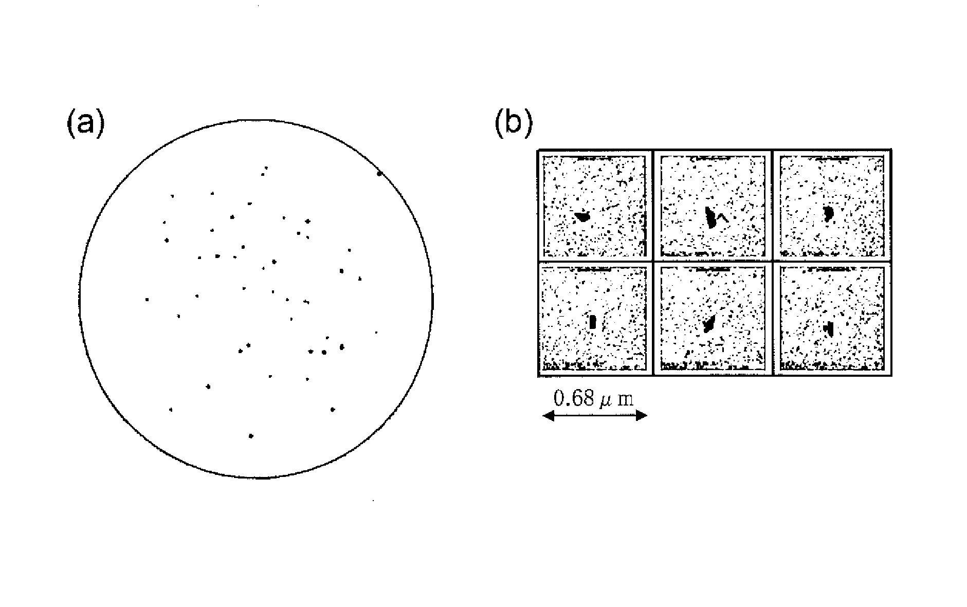
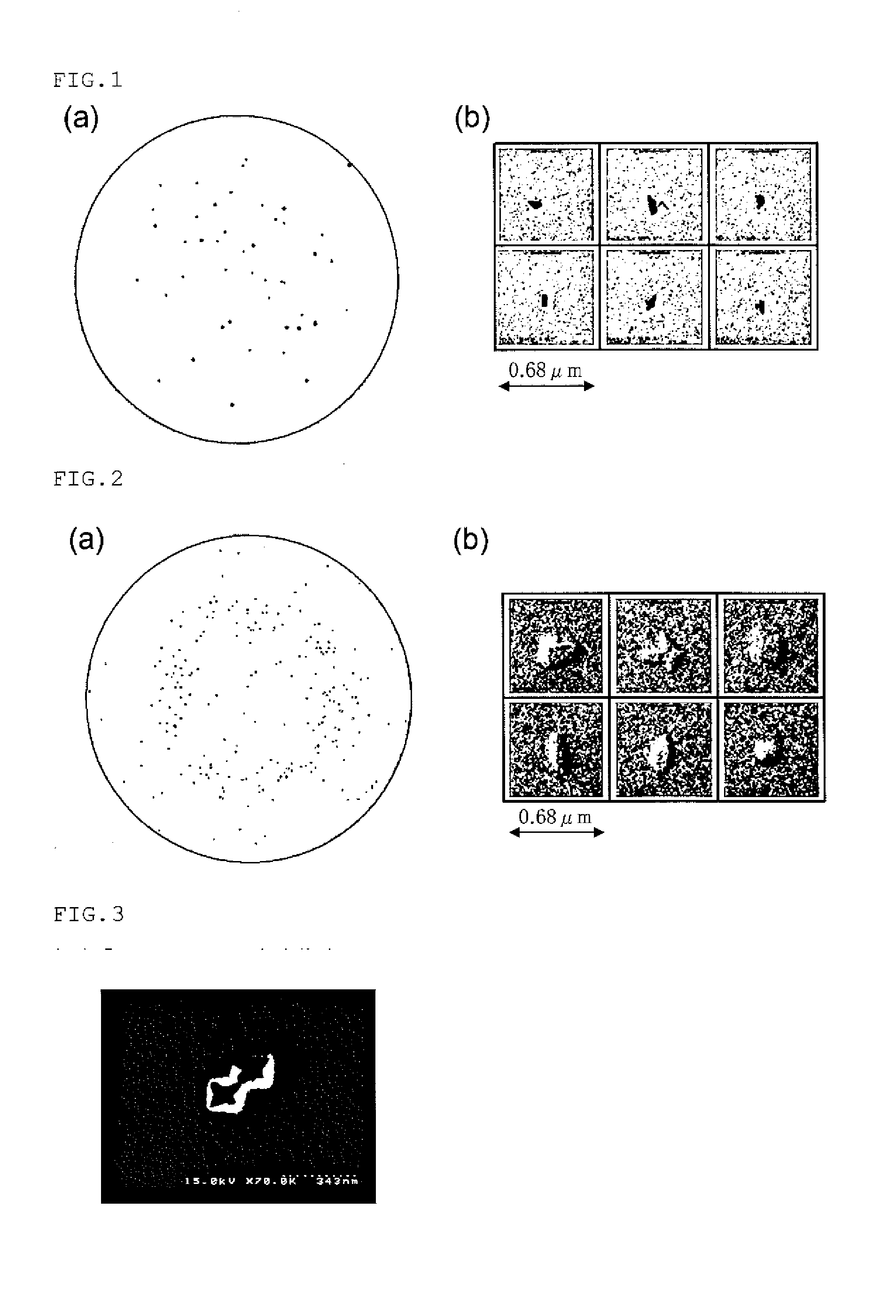
[0044]First, to determine a cause of generation of LPDs, a defect-free silicon single crystal of 300 mm in diameter was grown by filling a quartz crucible of 810 mm in diameter with 410 kg of polycrystalline silicon, melting the polycrystalline silicon, and then controlling a temperature gradient (G) and a growth rate (V) in a boundary region between a solid layer / a liquid layer of silicon as disclosed in Patent Literature 2. In doing so, boron doping was performed so that the resistivity became 10 Ω·cm, and the crystal axis orientation was set at . Slicing, lapping, etching, mirror-polishing, and the like which were industrially generally applied were performed on this defect-free silicon single crystal, whereby a mirror-polished wafer I was produced. This mirror-polished wafer I was measured by a particle counter (KLA-Tencor Corporation Model name=SP2 Detection particle diameter size: 0.037 μm or more). The detection result of an LPD map in a wafer plane is depicted in FIG. 1(a).

[...

experimental example 2

[0046]Next, a mirror-polished wafer II was produced from a defect-free silicon single crystal produced with a different quartz crucible in the same manner as in Experimental Example 1 described above, and LPDs were examined. A detected LPD map in a wafer plane is depicted in FIG. 2(a), and the observation results of the surface of the mirror-polished wafer II, the observation results obtained by the SEM, are depicted in FIG. 2(b). As depicted in FIG. 2(a), it was confirmed that LPDs were generated on the surface of the mirror-polished wafer II. Moreover, as depicted in FIG. 2(b), it was revealed that the shapes of the LPDs thus detected were convex hillocks. This difference in shape revealed that a cause of formation of LPDs in the mirror-polished wafer II was different from that of the mirror-polished wafer I.

experimental example 3

The Shape of a COP

[0047]It is known that a crystal defect is detected as an LPD. It has been reported that a COP (Crystal Originated Particle) is detected as an octahedral void defect (Non-patent Literature 3). To check if the defect shapes detected in the mirror-polished wafers I and II were related to the COP, a silicon single crystal of 300 mm in diameter was grown by doubling the crystal growth rate so that the COP was generated. Other growth conditions were the same as those of Experimental Example 1. The result obtained by observing the shape of an LPD of a mirror-polished wafer III by the SEM, the mirror-polished wafer III obtained by slicing this silicon single crystal and subjected to mirror-polishing, is depicted in FIG. 3. As depicted in FIG. 3, a defect caused by the COP was a void defect called what is termed a twin pit which is two partially-overlapping defects whose one side is surrounded in a [110] direction. This revealed that the defects of the mirror-polished wafe...


PUM


Abstract

The present invention provides a method for producing a silicon wafer from a defect-free silicon single crystal grown by a CZ method, the method comprising: preparing a silicon wafer obtained by slicing the defect-free silicon single crystal and subjected to mirror-polishing; then performing a heat treatment step of subjecting the mirror-polished silicon wafer to heat treatment at a temperature of 500° C. or higher but 600° C. or lower for 4 hours or more but 6 hours or less; and performing a repolishing step of repolishing the silicon wafer after the heat treatment step such that a polishing amount becomes 1.5 μm or more. Therefore, it is an object to provide a method by which a silicon wafer can be produced at a high yield, the silicon wafer in which LPDs are reduced to a minimum, the silicon wafer with a low failure-incidence rate in an inspection step and a shipment stage.

Description

TECHNICAL FIELD[0001]The present invention relates to a silicon wafer in which LPDs (Light Point Defects) on the surface thereof are reduced to a minimum and a method far producing the silicon wafer.BACKGROUND ART[0002]For a silicon wafer used as a material for producing a semiconductor device, a substrate obtained by slicing a silicon single crystal grown by the Czochralski (CZ) method, in particular, the Magnetic field applied Czochralski (MCZ) method that produces a crystal while applying a magnetic field, the substrate with a polished surface, is used. In recent years, a wafer without slight projections and depressions has been required as the quality of the surface of such a wafer as the design rules in the production of the semiconductor device have become finer. This has become an increasingly important quality item for monitoring a break by slight projections and depressions and a foreign substance in a device production step because the size of wiring in device production h...

Claims


Application Information

Patent Timeline
IPC IPC(8): H01L21/02H01L29/34
CPCH01L29/34H01L21/02024C30B15/203C30B29/06C30B33/00C30B33/02H01L21/3221H01L29/30H01L21/322C30B15/00C30B15/14C30B15/20
Inventor FUSEGAWA, IZUMIHOSHI, RYOJISONOKAWA, SUSUMUSAITO, HISAYUKI
Owner SHIN-ETSU HANDOTAI CO LTD
Learn More