
Ge-based nmos device and method for fabricating the same

a technology of nmos and schottky mos, which is applied in the direction of semiconductor devices, basic electric elements, electrical equipment, etc., can solve the problems of reducing the resistance of source/drain, the electron barrier severely limits the improvement of the performance of the and the ge-based schottky mos transistor also has some problems to be solved, so as to reduce the electron barrier, improve the performance of the g

Active Publication Date: 2014-05-01
SEMICON MFG INT (SHANGHAI) CORP +1
View PDF1 Cites 21 Cited by
  • Summary
  • Abstract
  • Description
  • Claims
  • Application Information

AI Technical Summary

Benefits of technology

The present invention provides a method for improving the performance of a Ge-based Schottky NMOS transistor by depositing a double-layer dielectric thin film formed by germanium oxide and metal oxide between the source / drain region and the substrate. This method can alleviate the Fermi level pinning effect, decrease the electron barrier, and improve the transistor's performance. The thin layer of metal oxide overcomes the Fermi level pinning effect and reduces the electron barrier through the formation of interface dipoles. The metal oxide and GeO2 interface also blocks the Metal-Induced Gap States resulting in a further reduction of the electron Schottky barrier height. The ratio between the areal density of oxygen of the metal oxide and that of GeO2 is important, with larger metallic cation radius generating stronger dipoles for effective modulation of the Schottky barrier. The use of double-layer dielectric thin film formed by germanium oxide and metal oxide is more effective in adjusting the Schottky barrier and improving the transistor's performance as compared to a single layer of insulating dielectric material like aluminum oxide.

Problems solved by technology

Under the Moore Law, the integration density of conventional Si-based MOS device is continually raised, while it is also faced various challenge and limitation, such as, mobility degradation, carrier velocity saturation and DIBL effect and so on, in which the mobility degradation becomes one of the critical factors affecting the of further improvement of device performance.
Secondly, the substitution of the conventional highly doped source / drain with a Schottky source / drain structure not only avoids the problems of low solid solubility and rapid diffusion of impurities in the Ge material, but also decreases resistances of the source / drain.
However, the Ge-based Schottky MOS transistor also has some problems to be solved.
The high electron barrier severely limits the improvement of the performance of the Ge-based Schottky MOS transistor.
A higher barrier of the source / channel in on-state limits a current drive ability of the device, and a lower barrier of the source / channel in off-state leads to increasing of a leakage current of the device.

Method used


Image

  • Ge-based nmos device and method for fabricating the same
  • Ge-based nmos device and method for fabricating the same
  • Ge-based nmos device and method for fabricating the same

Examples


Embodiment Construction

[0025]The embodiments of the present invention are further described below with combination of the attached drawings and specific embodiments.

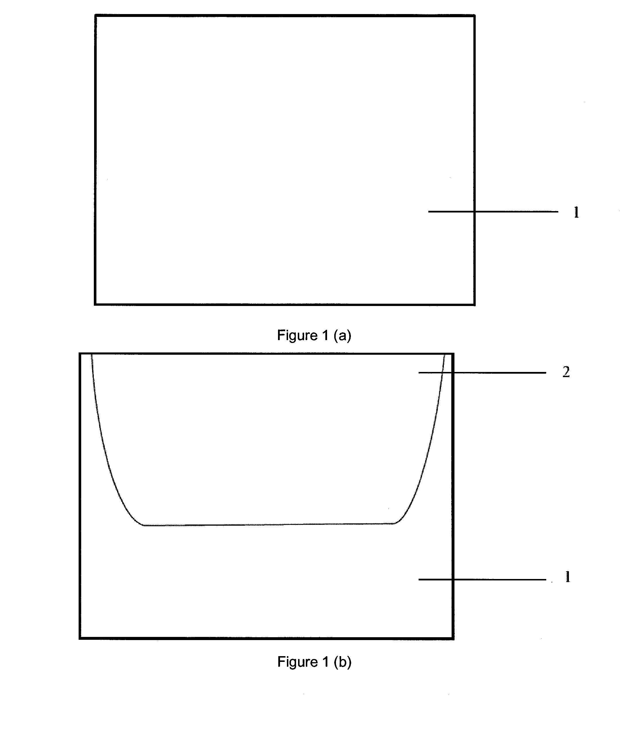
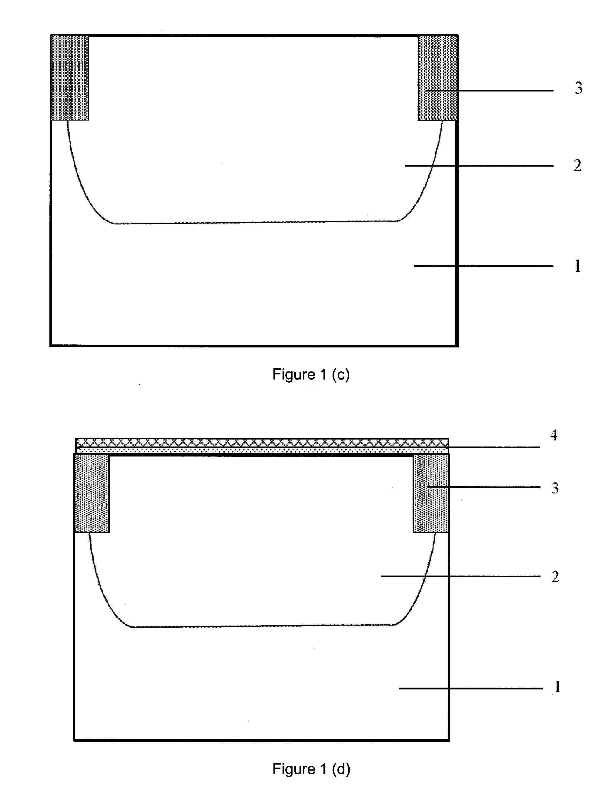
[0026]FIG. 1 shows a flow of a method for fabricating the Ge-based Schottky transistor of a preferred embodiment of the present invention. The method for fabricating the Ge-based Schottky transistor of the preferred embodiment of the present invention includes the following steps:

[0027]Step 1: a Ge-based substrate is provided. As shown in FIG. 1(a), the Ge-based substrate may be an N type semiconductor Ge substrate 1, wherein, the substrate 1 may be a bulk Ge, a Ge-on-insulator (GOI) or an epitaxial Ge substrate or the like.

[0028]Step 2: a P-type well region is formed. A silicon oxide layer and a silicon nitride layer are deposited over the Ge substrate. The P type well region is firstly defined by a photolithography process and the silicon nitride in the P-typed well region is ion-reaction etched. Subsequently, P type impurities such as B are...


PUM

PropertyMeasurementUnit
thicknessaaaaaaaaaa
thicknessaaaaaaaaaa
areal densityaaaaaaaaaa

Abstract

The embodiments of the present invention provide a Ge-based NMOS device structure and a method for fabricating the same. By using the method, double dielectric layers of germanium oxide (GeO2) and metal oxide are deposited between the source / drain region and the substrate. The present invention not only reduces the electron Schottky barrier height of metal / Ge contact, but also improves the current switching ratio of the Ge-based Schottky and therefore, it will improve the performance of the Ge-based Schottky NMOS transistor. In addition, the fabrication process is very easy and completely compatible with the silicon CMOS process. As compared with conventional fabrication method, the Ge-based NMOS device structure and the fabrication method in the present invention can easily and effectively improve the performance of the Ge-based Schottky NMOS transistor.

Description

CROSS-REFERENCES TO RELATED APPLICATION[0001]The present application claims priority to Chinese patent application (application number NO. 201110170991.4), filed to State Intellectual Property Office of China on Jun. 23, 2011, which is incorporated entirely herein by reference.FIELD OF THE INVENTION[0002]The present invention relates to the field of the ultra large scaled integrated circuit (ULSI) fabrication technologies, and in particular, to a structure of a germanium-based NMOS device and a method for fabricating the same.BACKGROUND OF THE INVENTION[0003]Under the Moore Law, the integration density of conventional Si-based MOS device is continually raised, while it is also faced various challenge and limitation, such as, mobility degradation, carrier velocity saturation and DIBL effect and so on, in which the mobility degradation becomes one of the critical factors affecting the of further improvement of device performance. In order to solve these problems resulting from the sca...

Claims


Application Information

Patent Timeline
Patent Type & Authority Applications(United States)
IPC IPC(8): H01L29/51H01L29/66H01L29/78H10B12/00
CPCH01L29/78H01L29/0895H01L29/41783H01L29/16H01L29/66643H01L29/66477H01L29/517
Inventor HUANG, RULI, ZHIQIANGAN, XIAGUO, YUEZHANG, XING
Owner SEMICON MFG INT (SHANGHAI) CORP
Learn More