

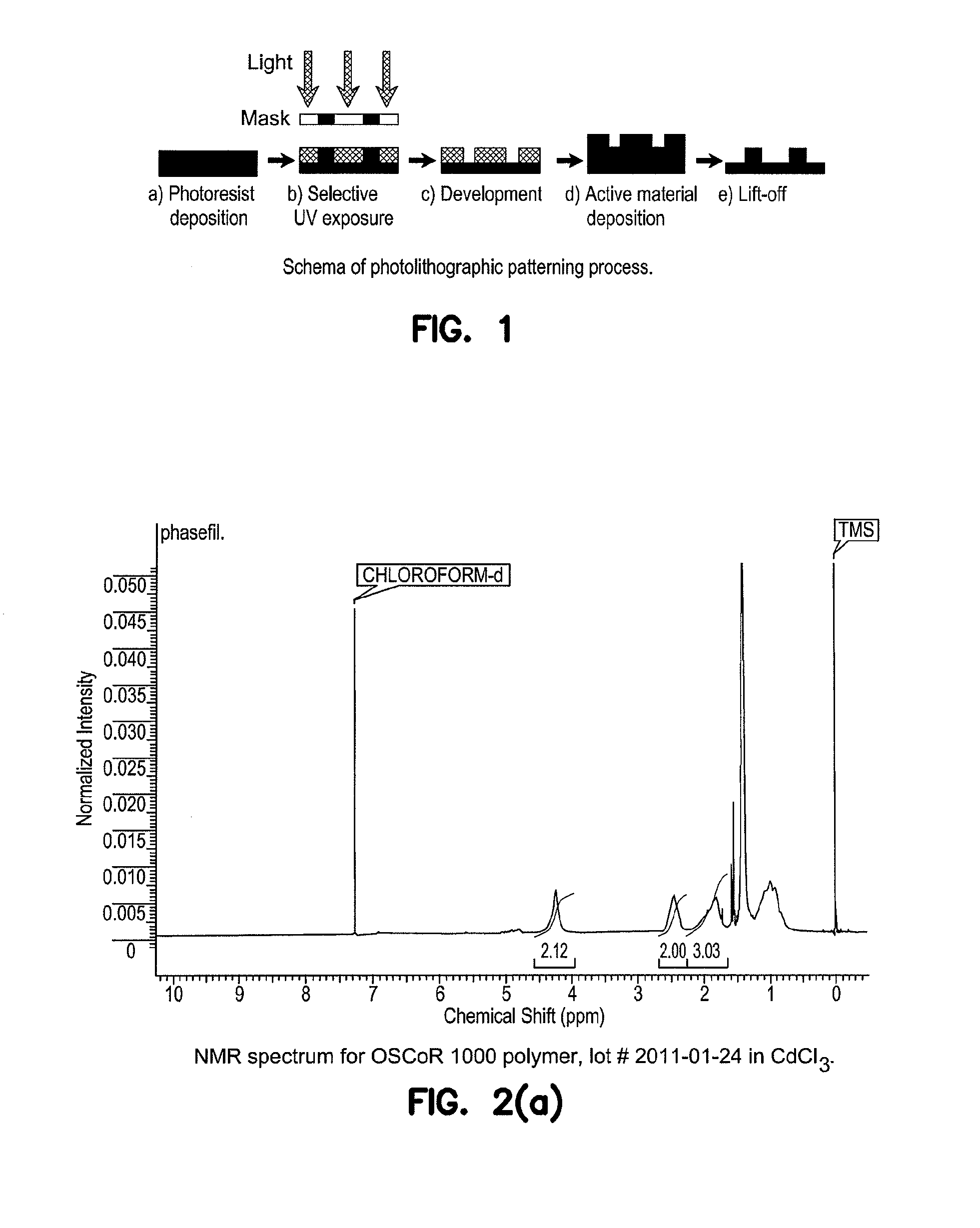
Orthogonal solvents and compatible photoresists for the photolithographic patterning of organic electronic devices
a technology of organic electronic devices and solvents, applied in the direction of photosensitive materials, photomechanical devices, instruments, etc., can solve the problems of organic materials that are much less resistant to solvents, organic electronics are degraded by conventional lithographic solvents and processes, and hinder the development of devices based on these materials
- Summary
- Abstract
- Description
- Claims
- Application Information
AI Technical Summary
Benefits of technology
Problems solved by technology
Method used
Image

Examples
example 1
Preparation of FOMA-TBMA Photoresist
[0071]A solution of 110.10 g (0.7743 mol.) of tert-butyl methacrylate, (TBMA), 330.07 g (0.7636 mol.) of 1H,1H,2H,2H-perfluorooctyl methacrylate, (“FOMA”), 874.2 g of Novec 7600 and 5.51 g (0.0335 mol.) of azobisisobutyronitrile, (“AIBN”) was stirred in a jacketed reaction flask. The flask jacket was connected to a programmable, constant temperature bath (“CTB”) capable of heating and maintaining a set jacket temperature. The solution was sparged with nitrogen at a rate of 0.5 L / minute for 1 hour at ambient temperature. A CTB program was initiated which heated the reaction jacket to 68° C., holds this temperature for 1 hour, heats to 72° C. and holds for 1 hour, and finally heats to 76° C. and holds for 12 hours. When the heating program was completed, the CTB was set to cool the reaction mixture to ambient temperature. The clear, colorless polymer solution obtained was diluted to a viscosity by the addition of 3.714 kg of Novec™ 7600, and a small...
example 2
Characterization of FOMA-TBMA Photoresist
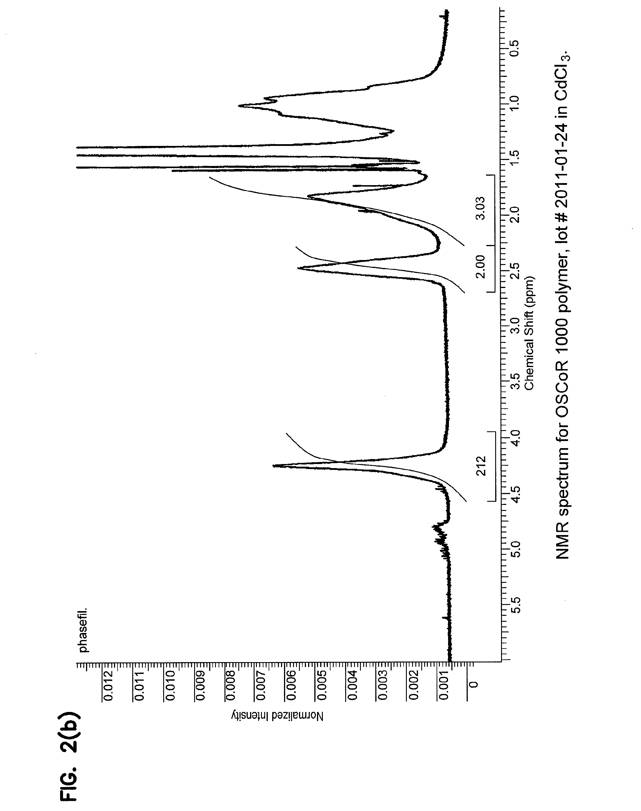
[0072]Proton NMR was performed on the photoresist sample obtained from Example 1 resuspended in deuterated chloroform (CdCl3), with the resulting spectrum obtained from this sample shown in FIGS. 2(a) and 2(b). In this spectrum, the broad peak centered at 2.5 ppm arises from the methylene group adjacent to the perfluoroalkyl chain in the FOMA, while the broad peak centered at 1.7 ppm arises from the TBMA methyl group in the polymer backbone. Proton integration (red overlay) of these peaks was used to calculate a mole ratio of the monomers in the photoresist polymer as FOMA / TBMA: 1.00 / 1.01, which closely matches the input (feed) FOMA / TBMA monomer ratio of 1.000 / 1.014.
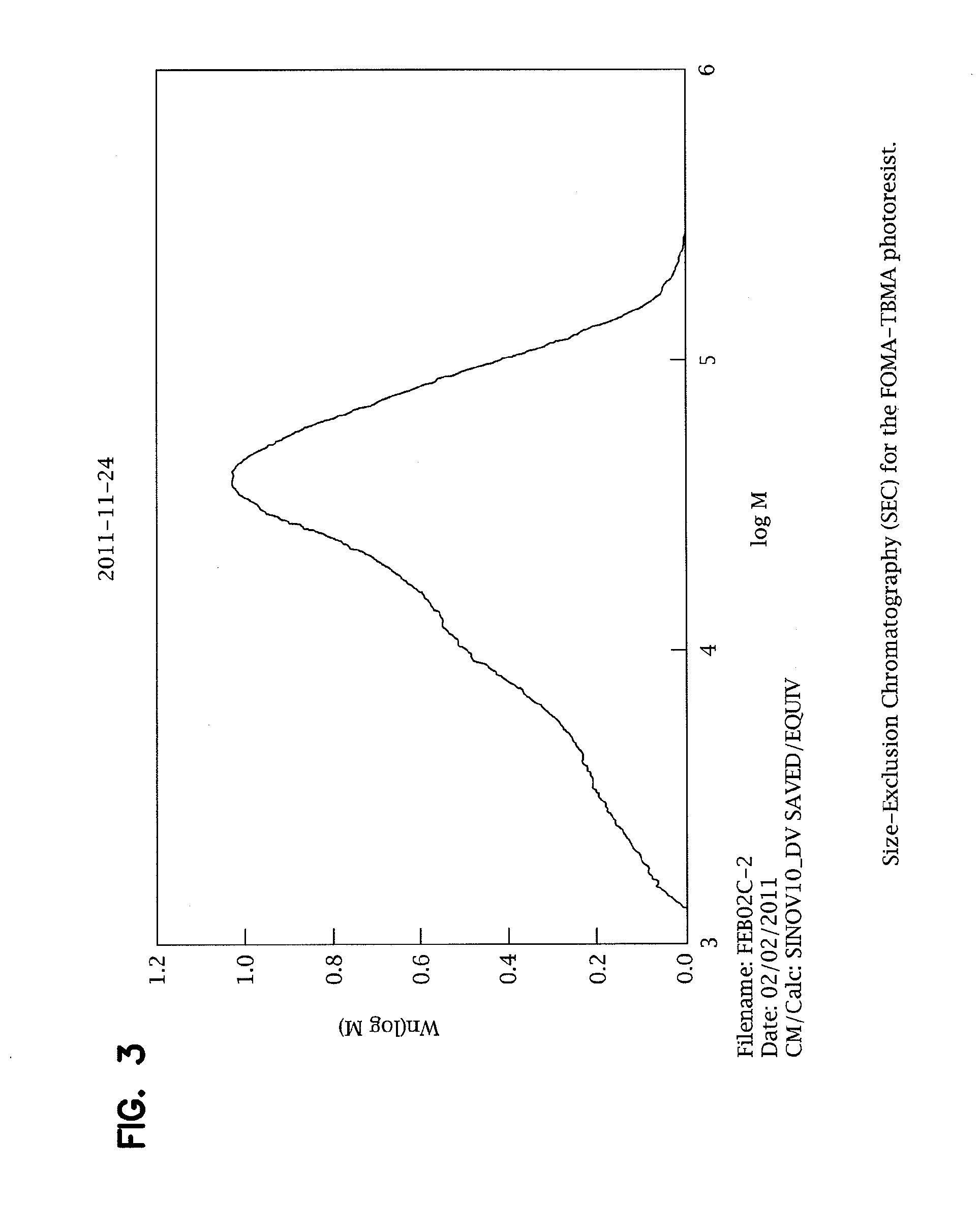
[0073]In order to determine the size distribution of the photoresist polymer, size-exclusion chromatography (SEC) was performed, as is shown in FIGS. 3 and 4, yielding a weight-averaged molecular weight of Mw=37,300. Glass transition temperature analyses were also performed, with ...
example 3
Patterning of FOMA-TBMA Photoresist
[0074]PAG-containing FOMA-TBMA photoresist prepared as described in Example 1 was deposited on substrate using spin coating. Specifically, spin coating was performed with a static dispense method, where photoresist was placed on a non-spinning wafer and the wafer was rapidly (<2 seconds) brought up to full rotational speed. Spin coating in all cases was done for 60 seconds with a covered spin coater (Cee Processing equipment from Brewer Science) in a fume hood to control airflow and particle contamination. Films were measured with a FilMetrics F50 thickness mapping tool, using index values measured on a Woolam Elipsometer. FIG. 5 provides a spin curve for FDMA-TBMA.
[0075]After spin-coating, the coated substrate was baked at 90° C. for 1 minute.
[0076]The coated substrate was then exposed to 365 nm (“I-line”) light, typically in a dose range of between 50 and 80 mJ / cm2, and then subjected to a post-exposure bake (“PEB”) step. For a 75° C. PEB, the pr...
PUM
| Property | Measurement | Unit |
|---|---|---|
| molecular weight distribution | aaaaa | aaaaa |
| thickness | aaaaa | aaaaa |
| wavelength | aaaaa | aaaaa |
Abstract
Description
Claims
Application Information