Method for manufacturing gallium nitride-based film chip

a technology of gallium nitride and film chip, which is applied in the direction of semiconductor devices, basic electric elements, electrical equipment, etc., can solve the problems of limiting the power of light-emitting devices, current congestion, and poor electrical conductivity and heat dissipation, so as to reduce the tearing force of gan film, increase device yield, and ensure hardness and strength

Active Publication Date: 2014-05-29
SHINEON INNOVATION TECH CO LTD +1
View PDF4 Cites 10 Cited by
  • Summary
  • Abstract
  • Description
  • Claims
  • Application Information

AI Technical Summary

Benefits of technology

[0019]The present invention uses glues to transfer the epitaxial layer. Especially, bonding the epitaxial layer with the first temporary substrate using glue before laser lift-off, because the glue has appropriate strength and hardness, it can effectively reduce the tear strength of GaN films when removing the sapphire substrate by laser. So it can reduce the damage of gallium nitride thin films, and greatly improve the yield of the GaN-based thin film chip.
[0035]The present invention uses glue to remove the epitaxial layer, bonding the second temporary in the second transfer process, so the first temporary substrate and glue can be etched smoothly, it improves the production yield.
[0048]In the present invention, epitaxial layer is bonded with the permanent substrate, then adhesive is used to bond the permanent substrate with a temporary substrate, since the adhesive has a certain hardness and strength, it can reduce the tearing force of the GaN film, and increase the device yield.

Problems solved by technology

The sapphire substrate is the main substrate of growing GaN-based LED, but its electrical conductivity and heat dissipation are relatively poor.
The poor electrical conductivity forces traditional LED to adopt lateral structure, which causes the current congestion, and poor heat dissipation limits the power of light-emitting device.
Using laser tilt-off technique to remove the sapphire substrate to make a vertical structure LED can solve the problem of heat dissipation effectively, but the yield is usually very low.
In addition, the stress is from the difference in thermal expansion coefficient of sapphire, GaN films and the support substrate, so the GaN films are easily broken when sapphire substrate is removed.
But since the bonding interface is not smooth and the gap is small, there will be a pulling force to GaN films during the laser lift-off process and the damage and rupture of GaN films may occur.
A traditional method is used by bonding the epitaxial layer on the sapphire with the electrically and thermally conductive substrate directly and then removing the sapphire substrate, but the yield of the chips is very low.
And the method cannot solve the stress in the process of laser and leads to cracking of a large number of chips.

Method used


Image

  • Method for manufacturing gallium nitride-based film chip
  • Method for manufacturing gallium nitride-based film chip
  • Method for manufacturing gallium nitride-based film chip

Examples


first embodiment

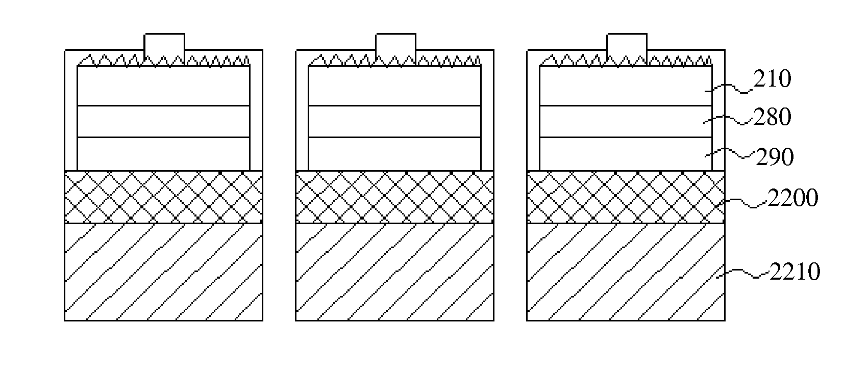
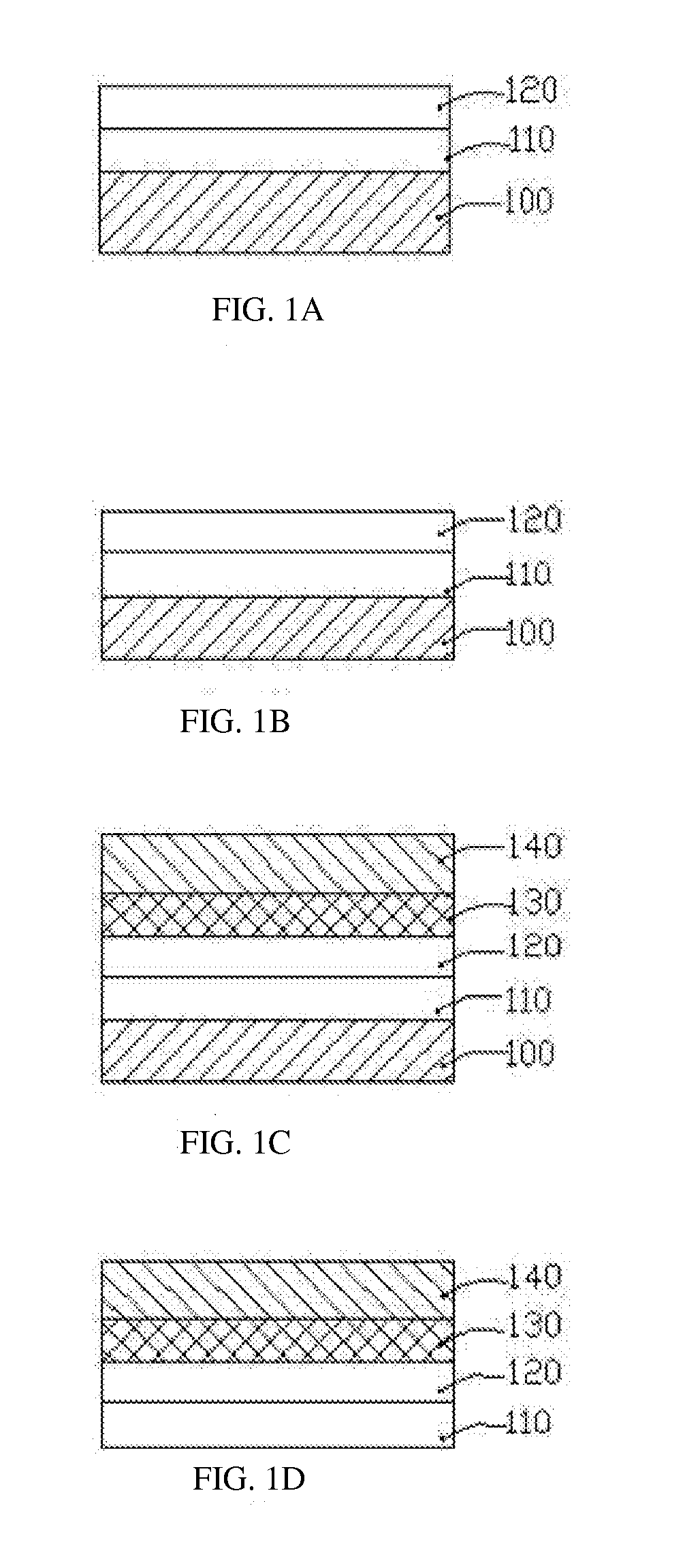
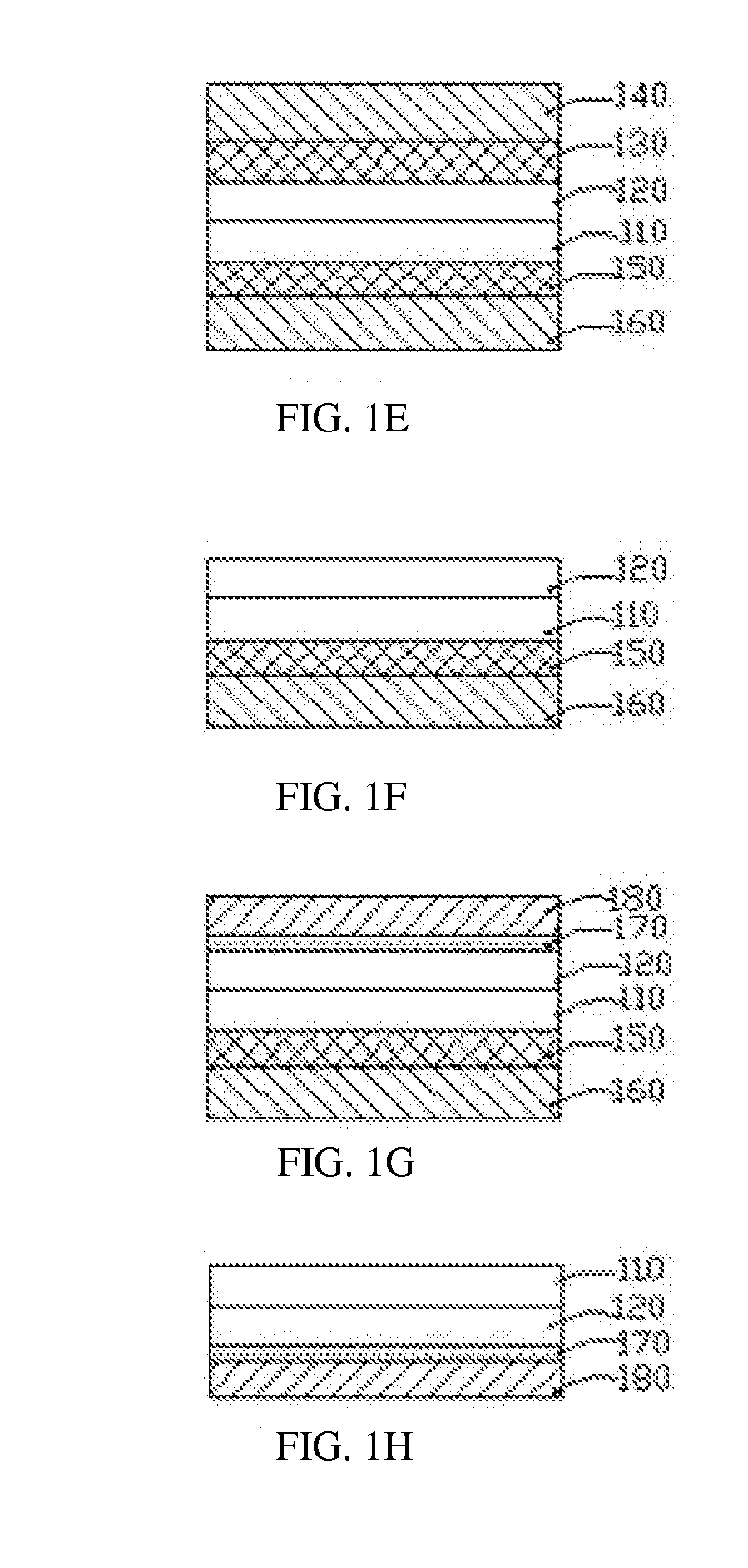
[0072]An n-type GaN layer, an active layer and a p-type GaN layer are grown in turn on the sapphire substrate by MOCVD. Ag as a reflective metal layer is formed on the epitaxial layer by electron beam evaporation. And then Cr / Pt / Au multilayer metal film is evaporated on the reflective metal layer and then alloyed at the temperature of 500° C. The thickness of the sapphire substrate is 120 microns by thinning and polishing. And then the sapphire substrate is periodically cut to obtain single components. The thickness of the first glue is about 25 microns. It is a modified epoxy resin adhesive and coated on the reflecting compound metal layer and solidified with a first temporary silicon substrate at the temperature of 100° C. for 60 minutes. After curing its shore hardness is between 80 D and 10 D, resistance temperature is from −25° C. to 300° C., bending strength is within a range from 80 MPa to 120 MPa and compressive strength is between 200 MPa and 300 MPa. The sapphire substrate...

second embodiment

[0073]An n-type GaN layer, an active layer and a p-type GaN layer are grown on the sapphire substrate. Ag as a reflective metal layer and Cr / Pt / Au multilayer metal film are formed by electron beam evaporation and then: alloyed at the temperature of 500° C. The thickness of the sapphire substrate is 150 microns by thinning and polishing. And then the sapphire substrate is periodically cut to obtain single components. A first glue about the thickness of 20 microns, a high temperature modified epoxy resin adhesive is coated on the reflecting compound metal layer and solidified with a first temporary silicon substrate at the temperature of 120° C. for 40 minutes. The sapphire substrate is lifted off by using the excimer laser at 193 nm and 480 mW. And then a second glue, the modified heterocyclic resin is coated on the newly exposed surface and solidified with a second temporary silicon substrate at the temperature of 120° C. for 60 minutes. Next when the second temporary silicon substr...

third embodiment

[0074]A buffer layer, an n-type GaN layer, an active layer and a p-type GaN layer are grown on the sapphire substrate by MOCVD. Ag / Pt as a reflecting compound metal layer is formed by electron beam evaporation and then alloyed at the temperature of 500° C. The thickness of the sapphire substrate is 400 microns by polishing after the epitaxial wafer is coated by wax. And then the sapphire substrate is periodically cut to obtain single components. A first glue about the thickness of 60 microns, a high temperature modified epoxy resin adhesive is coated on the reflecting compound metal layer and solidified with a temporary sapphire substrate at the temperature of 120° C. for 60 minutes. And then the sapphire substrate is removed by using the excimer laser at 248 nm and 550 mW. And a second glue, a modified heterocyclic resin is coated on the peeling surface and solidified with a temporary silicon substrate at the temperature of 120° C. for 60 minutes. Next, when the second glue is prot...


PUM

PropertyMeasurementUnit
temperatureaaaaaaaaaa
compressive strengthaaaaaaaaaa

Abstract

A method for manufacturing gallium nitride-based film chip is provided. The method comprises: growing a gallium nitride-based semiconductor multilayer structure on a sapphire substrate; thinning and polishing the sapphire substrate; coating a reflecting compound metal layer on the gallium nitride-based semiconductor multilayer structure by evaporating; coating a first glue on the reflecting compound metal layer and solidifying the first glue with a first temporary substrate; peeling the sapphire substrate off by laser; coating a second glue on the peeling surface and solidifying the second glue with a second temporary substrate; removing the first temporary substrate and the first glue; bonding the reflecting compound metal layer with a permanent substrate by eutectic bonding; removing the second temporary substrate and the second glue.

Description

CROSS-REFERENCE TO RELATED APPLICATIONS[0001]This is a continuation of International Application PCT / CN2012000664, with an international filing date of May 15, 2012, which has a priority date of May 19, 2011, claiming benefits of China applications 201110132402.3, 201110132423.5, and 201110132454.0.BACKGROUND OF THE INVENTION[0002]1. Field of the Invention[0003]The present invention relates to processes for fabricating a semiconductor light-emitting device. More specifically the present invention relates to a method of fabricating GaN-based thin-film chips using laser ablation.[0004]2. Description of Related Art[0005]The sapphire substrate is the main substrate of growing GaN-based LED, but its electrical conductivity and heat dissipation are relatively poor. The poor electrical conductivity forces traditional LED to adopt lateral structure, which causes the current congestion, and poor heat dissipation limits the power of light-emitting device. Using laser tilt-off technique to rem...

Claims


Application Information

Patent Timeline
Patent Type & Authority Applications(United States)
IPC IPC(8): H01L21/02H01L21/762
CPCH01L21/0254H01L21/76256H01L21/02664H01L21/0242H01L33/0095H01L33/405H01L2221/68381H01L21/6835H01L2221/6835H01L2221/68368H01L33/0093
Inventor ZHAO, HANMINZHU, HAOXIONG, CHUANBINGQU, XIAODONG
Owner SHINEON INNOVATION TECH CO LTD
Why Eureka
Try Eureka