

Peeling method, semiconductor device, and peeling apparatus
a peeling apparatus and semiconductor technology, applied in the field of peeling methods, can solve the problems of high stress applied to the semiconductor element, and breakage of the semiconductor element in some cases, and achieve the effects of improving peelability, increasing yield in peeling steps, and increasing yield in manufacturing flexible devices
- Summary
- Abstract
- Description
- Claims
- Application Information
AI Technical Summary
Benefits of technology
Problems solved by technology
Method used
Image

Examples
embodiment 1
[0053]In this embodiment, an example of a peeling method of one embodiment of the present invention is described with reference to drawings.
[Example of Manufacturing Method]
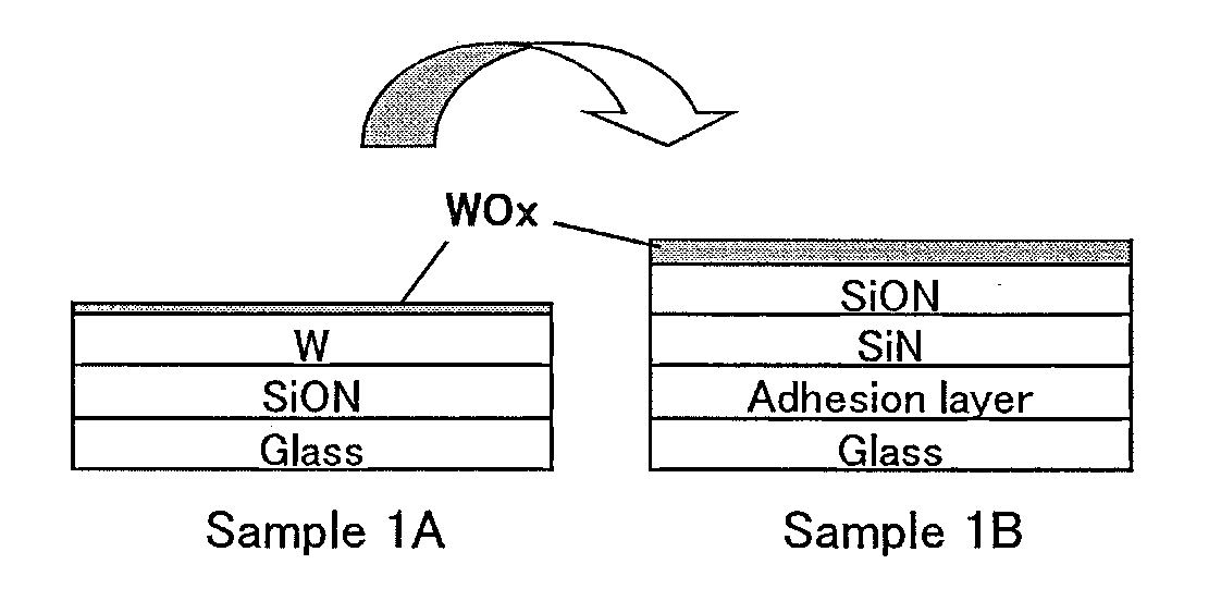
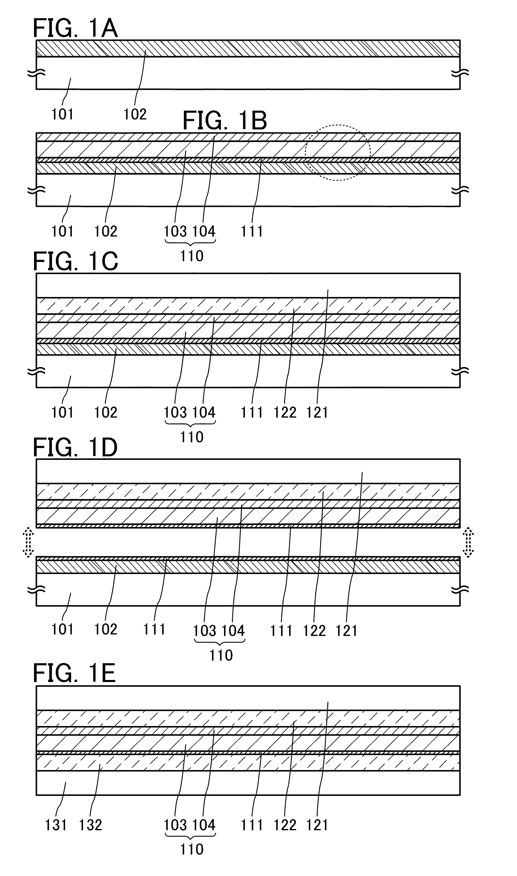
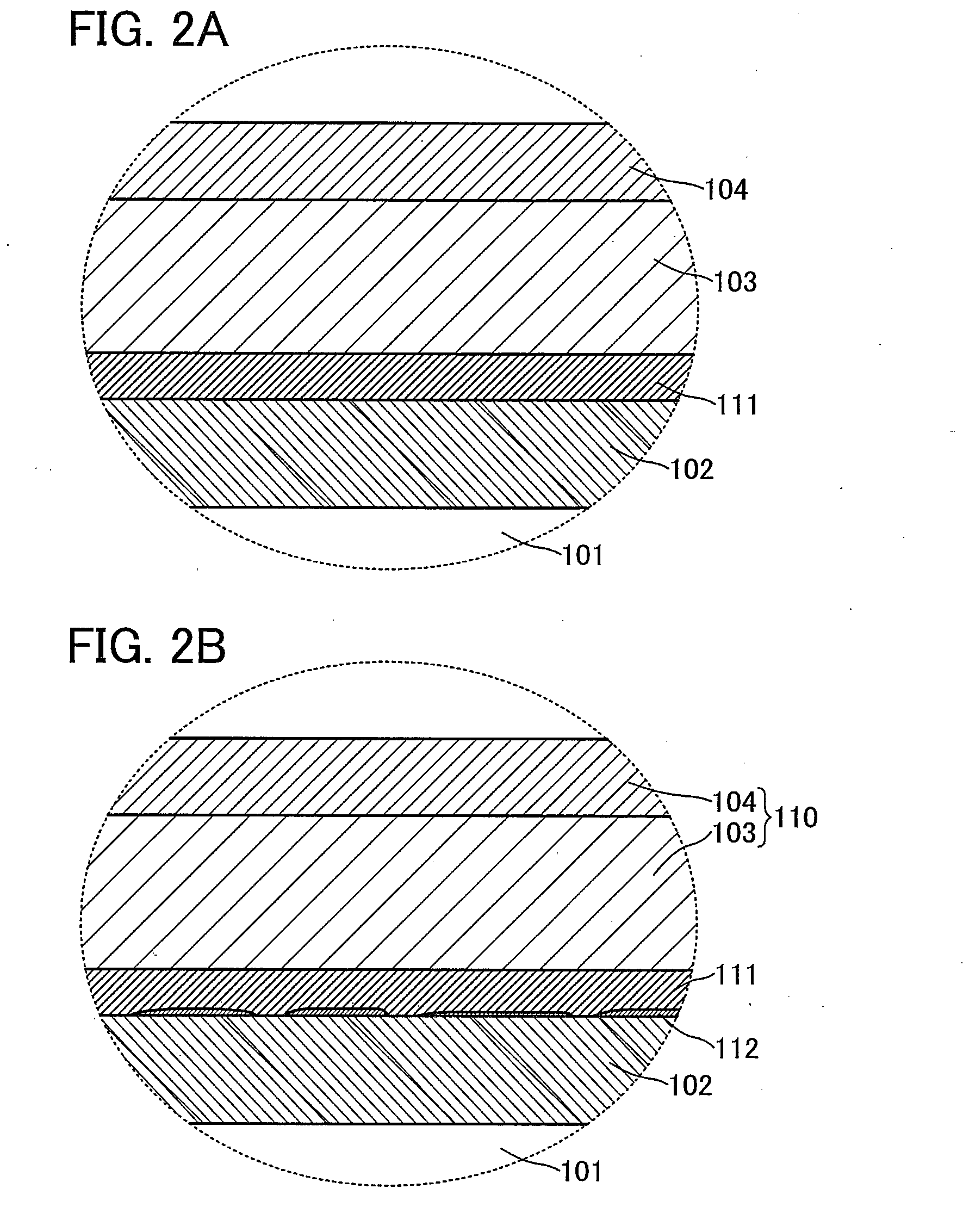
[0054]First, a peeling layer 102 is formed over a support substrate 101 (FIG. 1A).
[0055]A substrate which has resistance high enough to withstand at least heat in a later step is used as the support substrate 101. Examples of the support substrate 101 include a semiconductor substrate, a metal substrate, and a ceramic substrate in addition to a glass substrate and a resin substrate.
[0056]A high melting point metal such as tungsten, titanium, or molybdenum can be used for the peeling layer 102. Tungsten is preferably used.
[0057]The peeling layer 102 can be formed by, for example, a sputtering method. The thickness of the peeling layer 102 is greater than or equal to 10 nm and less than or equal to 200 nm, preferably greater than or equal to 20 nm and less than or equal to 100 nm.
[0058]Next, a layer 110 to be peele...
application example
[Application Example]
[0106]The peeling method described in the Example of Manufacturing Method can be applied to a variety of flexible devices.
[0107]In the case where the peeling method is applied to, for example, a flexible device including a transistor, the transistor may be formed after the layer 110 to be peeled is formed.
[0108]For example, in the case where a bottom-gate transistor is manufactured, a gate electrode, a gate insulating layer, a semiconductor layer, and a source and drain electrodes are formed in this order over the layer 110 to be peeled. After that, a step of bonding the substrate 121, a peeling step, and a step of bonding the substrate 131 are performed. In such a manner, a flexible device including the transistor can be manufactured.
[0109]Note that a forward staggered transistor, an inverted staggered transistor, or the like may be used. In addition, a top-gate transistor or a bottom-gate transistor may be used. In addition, a channel-etched transistor or a ch...
embodiment 2
[0117]In this embodiment, a flexible device which can be manufactured by the peeling method of one embodiment of the present invention is described with reference to drawings. Light-emitting devices such as an image display device (hereinafter, a display device) including an organic EL element and a lighting device are described as examples of the flexible device.
[0118]Note that a light-emitting device in this specification refers to an image display device or a light source (including a lighting device). In addition, the light-emitting device may include any of the following modules in its category: a module in which a connector such as a flexible printed circuit (FPC) or a tape carrier package (TCP) is attached to a light-emitting device; a module having a TCP provided with a printed wiring board at the end thereof; a module having an integrated circuit (IC) directly mounted over a substrate over which a light-emitting element is formed by a chip on glass (COG) method; a module in...
PUM
| Property | Measurement | Unit |
|---|---|---|
| Temperature | aaaaa | aaaaa |
| Temperature | aaaaa | aaaaa |
| Angle | aaaaa | aaaaa |
Abstract
Description
Claims
Application Information