Semiconductor device and method for producing semiconductor device

a semiconductor and semiconductor technology, applied in the direction of semiconductor devices, basic electric elements, electrical equipment, etc., can solve the problems of not disclosing a method of appropriately adjusting not disclosing a method of supplementing the amount of crystal defects to so as to improve the electrical characteristics, optimally control the amount of crystal defects, and increase the donor generation rate

Active Publication Date: 2014-09-04
FUJI ELECTRIC CO LTD
View PDF3 Cites 58 Cited by
  • Summary
  • Abstract
  • Description
  • Claims
  • Application Information

AI Technical Summary

Benefits of technology

[0024]According to the invention, the electron beam irradiation is performed before or after the proton implantation and the amount of crystal defects is optimally controlled during a heat treatment. Therefore, it is possible to increase the donor generation rate. In addition, according to the invention, when the heat treatment for generating donors ends, the crystal defects formed by the electron beam irradiation and the proton implantation are recovered and controlled to an appropriate amount of crystal defects. Therefore, it is possible to improve electrical characteristics. For example, it is possible to increase a breakdown voltage and reduce a leakage current.
[0025]According to the semiconductor device and the method for producing a semiconductor device of the invention, it is possible to increase the donor generation rate using proton implantation and improve the electrical characteristics.

Problems solved by technology

Patent Literature 1 discloses the degree of recovery of the crystal defects generated during proton implantation by the heat treatment, but does not disclose a method of supplementing the amount of crystal defects to increase the donor generation rate when the crystal defects generated during proton implantation are insufficient.
Patent Literature 2 discloses the oxygen concentration required to increase the donor generation rate, but does not disclose a method of appropriately adjusting the amount of crystal defects to increase the donor generation rate.

Method used


Image

  • Semiconductor device and method for producing semiconductor device
  • Semiconductor device and method for producing semiconductor device
  • Semiconductor device and method for producing semiconductor device

Examples


embodiment 1

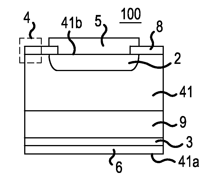
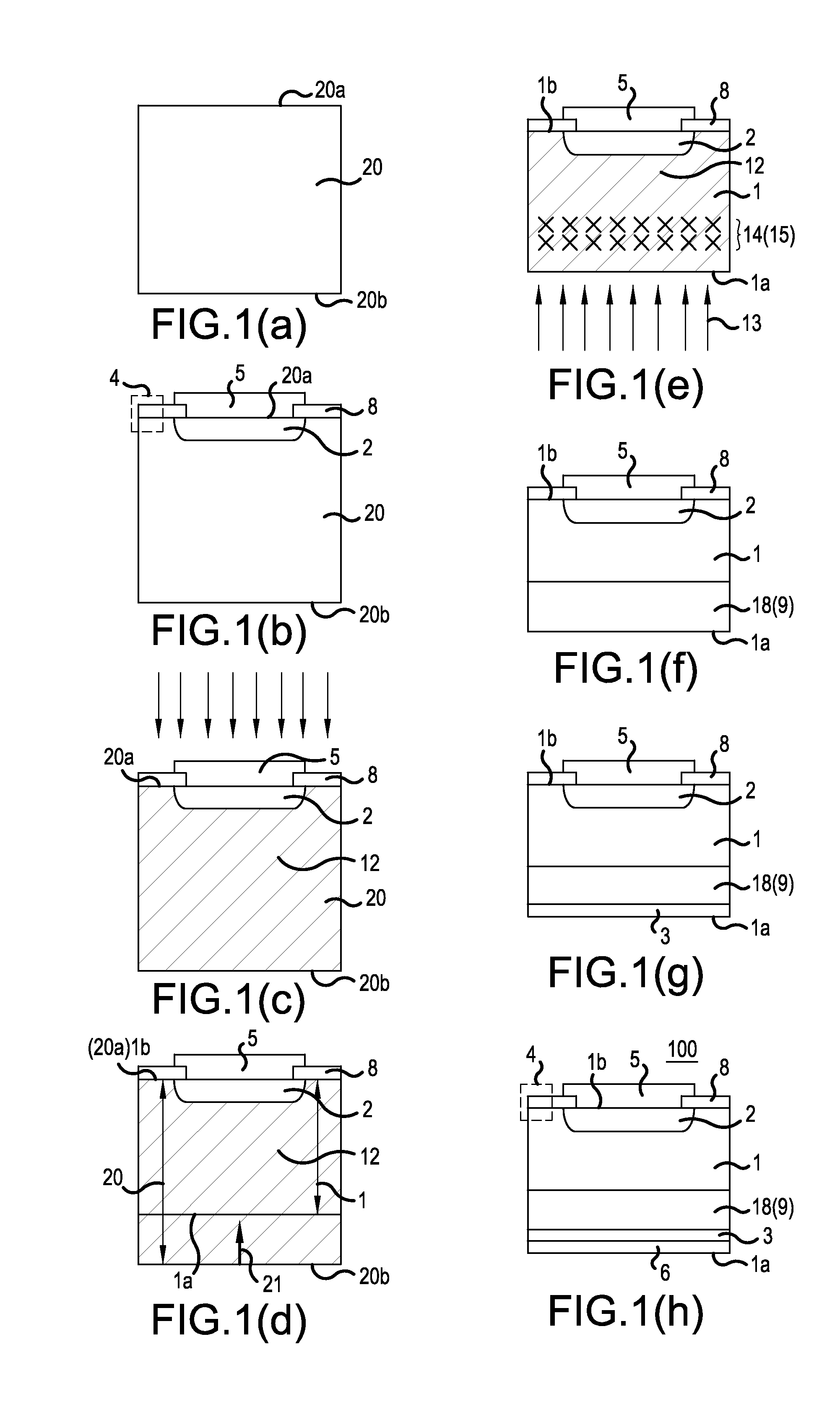
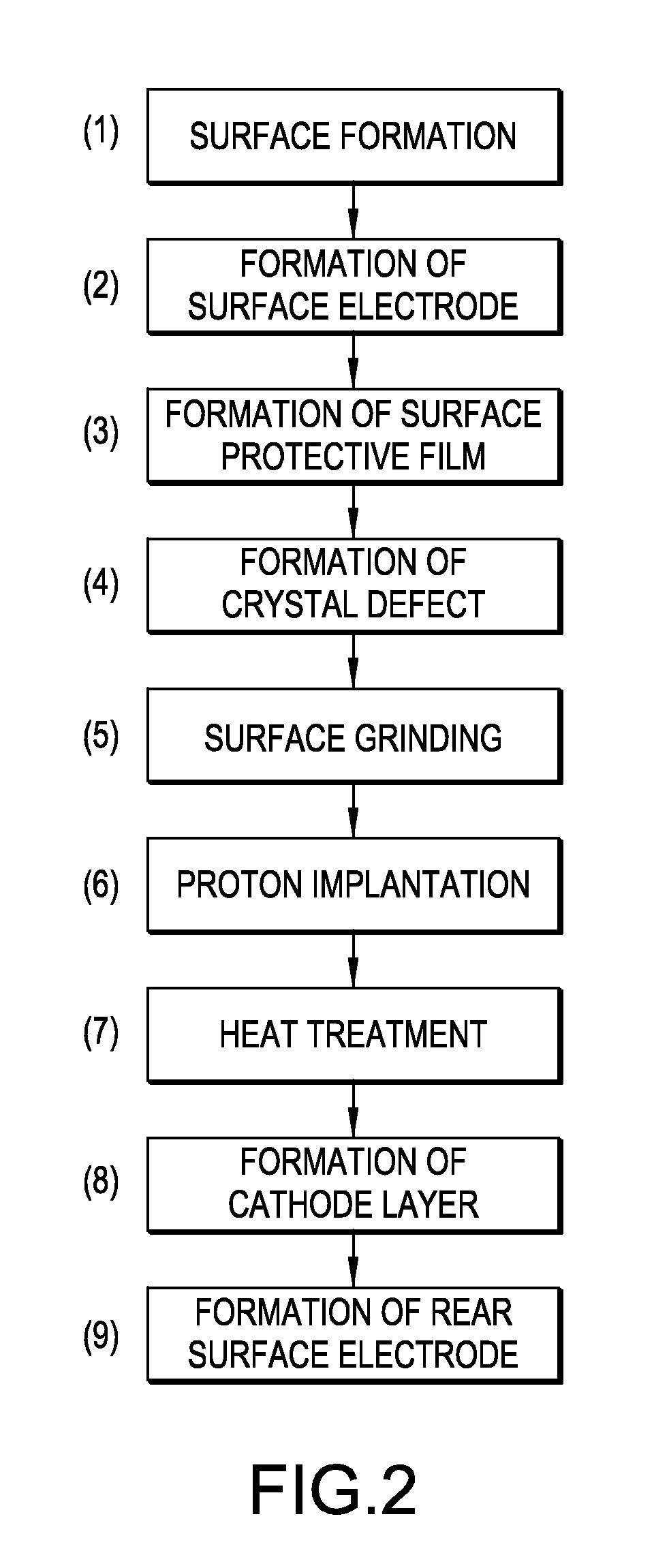
[0048]FIG. 1 is a cross-sectional view illustrating the sequence of a production process according to Embodiment 1 of the invention. FIG. 2 is a flowchart illustrating the flow of the production process shown in FIG. 1. Next, a method for producing a semiconductor device according to Embodiment 1 will be described with reference to FIGS. 1 and 2. The semiconductor device manufactured (produced) by the semiconductor device production method according to Embodiment 1 shown in FIG. 1 is diode 100 including n-type field stop (FS) layer 9 illustrated in FIG. 1(h). First, for example, an n-type silicon substrate is prepared as thick n− semiconductor substrate 20 which is not thinned (FIG. 1(a)).

[0049]Then, as illustrated in the processes (1) and (2) of FIG. 2, p-type anode region 2 and anode electrode 5 (metal) which is electrically connected to p-type anode region 2 are formed on a first main surface (front surface 20a) of n− semiconductor substrate 20, which will be an n− drift layer, b...

embodiment 2

[0074]FIG. 8 is a characteristic diagram illustrating a difference in carrier concentration distribution when electron beam irradiation is performed and when no electron beam irradiation is performed. FIG. 8(a) is a diagram illustrating the comparison between an example according to the invention in which electron beam irradiation is performed (hereinafter, referred to as an example) and an example according to the related art in which no electron beam irradiation is performed (hereinafter, referred to as Conventional example 1). FIG. 8(b) is a diagram illustrating the comparison between an example in which no electron beam irradiation is performed and Rp2 is equal to or more than 0.5Rp1 (hereinafter, referred to as Conventional example 2) and an example in which no electron beam irradiation is performed and Rp2 is less than 0.5Rp1 (Conventional example 1). Here, Rp1 and Rp2 are proton implantation ranges and are average ranges from rear surface 1a of n− semiconductor substrate 1. T...

embodiment 3

[0079]FIG. 9 is a flowchart illustrating the flow of a semiconductor device production process according to Embodiment 3. The semiconductor device production method according to Embodiment 3 is a modification of the semiconductor device production method according to Embodiment 1 in which the order of processes before and after proton implantation is changed. The semiconductor device production method according to Embodiment 3 differs from the semiconductor device production method according to Embodiment 1 in that, after a rear surface of an n− semiconductor substrate is ground and before proton implantation, ion implantation for forming a cathode layer is performed and the cathode layer is activated by laser annealing. The other processes in the semiconductor device production method according to Embodiment 3 are the same as those in the semiconductor device production method according to Embodiment 1.

[0080]Specifically, first, similarly to Embodiment 1, a surface forming process ...


PUM


Abstract

Hydrogen atoms and crystal defects are introduced into an n− semiconductor substrate by proton implantation. The crystal defects are generated in the n− semiconductor substrate by electron beam irradiation before or after the proton implantation. Then, a heat treatment for generating donors is performed. The amount of crystal defects is appropriately controlled during the heat treatment for generating donors to increase a donor generation rate. In addition, when the heat treatment for generating donors ends, the crystal defects formed by the electron beam irradiation and the proton implantation are recovered and controlled to an appropriate amount of crystal defects. Therefore, for example, it is possible to improve a breakdown voltage and reduce a leakage current.

Description

BACKGROUND OF THE INVENTION[0001]A. Field of the Invention[0002]The present invention relates to a semiconductor device and a method for producing a semiconductor device, and more particularly, to a semiconductor device, such as a diode or an insulated gate bipolar transistor (IGBT) including an n− type field stop layer, and a method for producing a semiconductor device.[0003]B. Description of the Related Art[0004]As a semiconductor device used in a power semiconductor device, for example, there is a diode or an IGBT with a breakdown voltage of 400 V, 600 V, 1200 V, 1700 V, 3300 V, or a higher one. The diode or the IGBT is used in a power conversion apparatus such as a converter or an inverter. The power semiconductor device requires good electrical characteristics, such as low loss, high efficiency, and a high breakdown voltage, and low costs. For example, a semiconductor device has been known in which a donor layer which will be an n-type field stop (FS) layer is provided in an n−...

Claims


Application Information

Patent Timeline
Patent Type & Authority Applications(United States)
IPC IPC(8): H01L29/32H01L29/861H01L29/10H01L29/739
CPCH01L29/32H01L29/1095H01L29/861H01L29/7395H01L21/263H01L21/26506H01L29/0834H01L29/36H01L29/66128H01L29/8611H01L29/0619H01L21/324H01L21/26513H01L29/063
Inventor YOSHIMURA, TAKASHIMIYAZAKI, MASAYUKITAKISHITA, HIROSHIKURIBAYASHI, HIDENAO
Owner FUJI ELECTRIC CO LTD
Why Eureka
Try Eureka