Supercharge Your Innovation With Domain-Expert AI Agents!

Polishing composition and polishing method using same, and substrate manufacturing method

a technology of composition and polishing method, applied in the field of polishing composition, can solve the problems of high hardness, difficult etching, and insufficient cmp rate of polishing materials for copper or copper alloys, and achieve the effect of inhibiting corrosive defects and high polishing ra

Inactive Publication Date: 2014-09-18
FUJIMI INCORPORATED
View PDF7 Cites 2 Cited by
  • Summary
  • Abstract
  • Description
  • Claims
  • Application Information

AI Technical Summary

Benefits of technology

The present invention reduces corrosion while maintaining a high polishing rate for objects that have a conductor layer and an electrically conductive material layer in contact with the conductor layer. This particularly applies to conductor layers containing a noble metal.

Problems solved by technology

The barrier layer conductor film, however, typically has a higher hardness comparing with copper or copper alloys, thus combination of the polishing materials for copper or copper alloys cannot provide a sufficient CMP rate in many cases.
On the other hand, tantalum, tantalum alloys, tantalum compounds and the like used as the barrier layer are chemically stable and are thus difficult to etch and cannot be mechanically polished as easily as copper and copper alloys due to the higher hardness.
Ruthenium, ruthenium alloys, and ruthenium compounds are, however, difficult to be polished due to high chemical stability and hardness thereof similarly to tantalum, tantalum alloys, and tantalum compounds.
A ruthenium film, however, has higher chemical stability and hardness than other metal films for damascene wiring such as copper or tungsten and is thus difficult to polish.
Therefore, the increase in the polishing rate for a ruthenium film results in increased defects on the metal film for damascene wiring.

Method used


Image

  • Polishing composition and polishing method using same, and substrate manufacturing method

Examples


Embodiment Construction

[0023]Embodiments of the present invention will be described below.

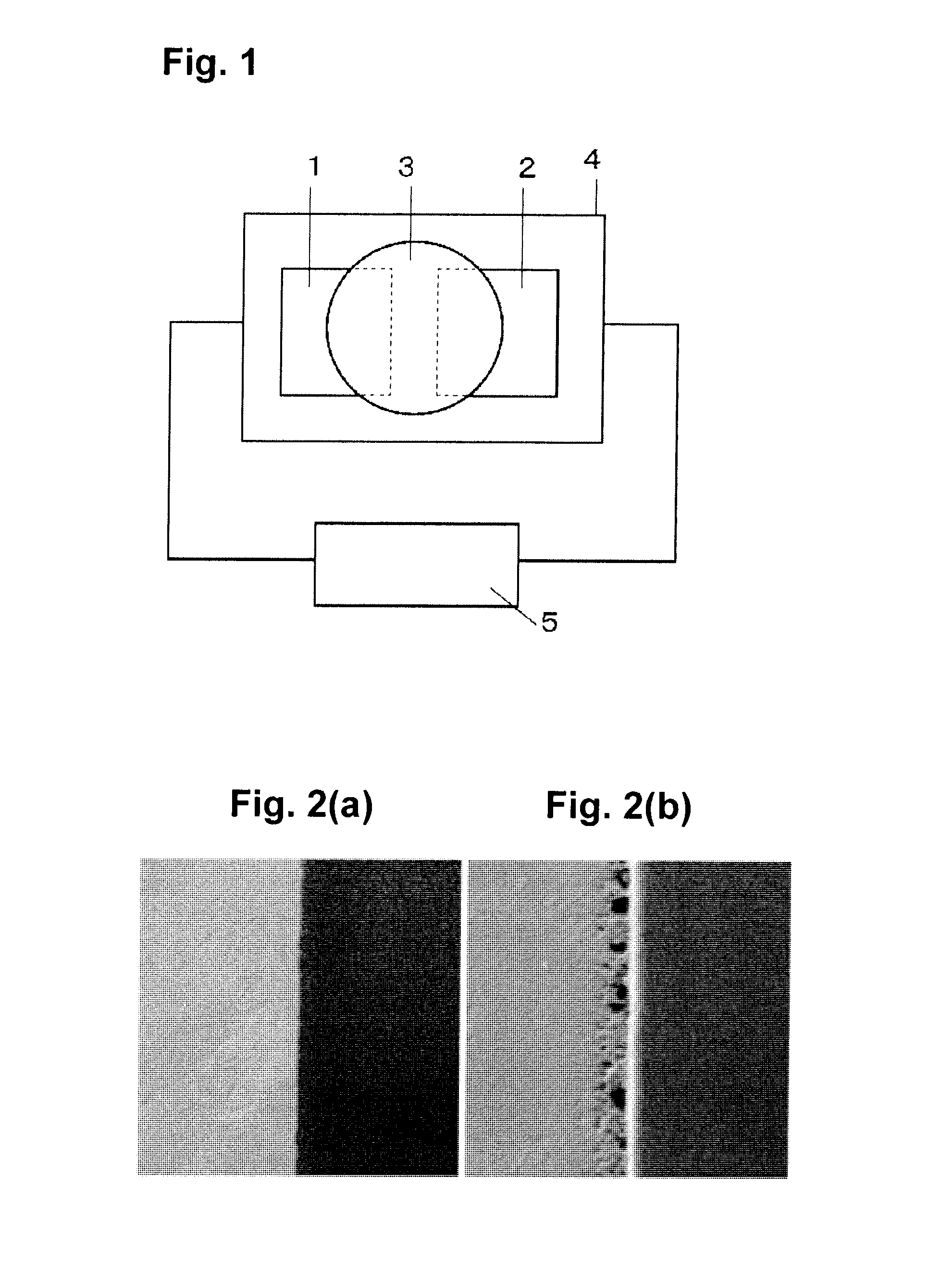
[0024]A polishing composition of the present embodiment is used for polishing an object including a conductor layer and an electrically conductive material layer that is in contact with the conductor layer. Examples of the object to be polished include a substrate used in the wiring part forming process for semiconductor devices, including an interlayer insulation film with recessed parts and projecting parts on the surface thereof, a barrier conductor layer covering the interlayer insulation film along with the surface thereof, and an electrically conductive material layer composed mainly of copper filled in the recessed parts to cover the barrier conductor layer.

[0025]Examples of the electrically conductive material include materials composed mainly of metal such as copper, a copper alloy, a copper oxide, a copper alloy oxide, tungsten, a tungsten alloy, silver, a silver alloy, and gold. Above all, electrically con...


PUM

PropertyMeasurementUnit
Temperatureaaaaaaaaaa
Electrical conductivityaaaaaaaaaa
Currentaaaaaaaaaa

Abstract

Provided is a polishing composition to be used for polishing an object including a conductor layer and an electrically conductive material layer that is in contact with the conductor layer. In a state in which the positive electrode and the negative electrode of an electrometer are connected to the electrically conductive material layer and the conductor layer, respectively, in the polishing composition at ordinary temperature, the current flowing from the positive electrode to the negative electrode has a positive value or is zero when the electrically conductive material layer and the conductor layer are polished. The polishing composition preferably contains a nitrogen atom-containing compound, a sulfur atom-containing compound, or a phosphorus atom-containing compound as an additive to control the value of the current to positive or zero.

Description

TECHNICAL FIELD[0001]The present invention relates to a polishing composition suitable for polishing noble metals and the use thereof.BACKGROUND ART[0002]In recent years, novel micromachining techniques have been developed accompanying high integration and high performance of LSIs. Chemical mechanical polishing (hereinafter referred to as “CMP”) method is one of those techniques and is often utilized in planarizing an interlayer insulation film, forming a metal plug, and forming embedded wiring (damascene wiring) in an LSI manufacturing process, particularly in a multilayer interconnection forming process. This technique is, for example, disclosed in Patent Document 1. The damascene wiring technique can lead to a simplified wiring process, as well as improved yield and reliability, and thus is expected to expand application thereof.[0003]Currently, with regard to the damascene wiring, copper is primarily used as a wiring metal in high speed logic devices because of its low resistanc...

Claims


Application Information

Patent Timeline
IPC IPC(8): H05K3/26C09G1/02
CPCC09G1/02H05K3/26B24B37/044C09K3/1436C09K3/1463H01L21/3212B23H5/08B24B1/00C09K13/06C09G1/04C09G1/00C09K3/1454C09G1/06H01L21/30625
Inventor KACHI, YOSHIHIROTANAKA, TOMOEUMEDA, TAKAHIRO
Owner FUJIMI INCORPORATED
Features
  • R&D
  • Intellectual Property
  • Life Sciences
  • Materials
  • Tech Scout
  • Unparalleled Data Quality
  • Higher Quality Content
  • 60% Fewer Hallucinations
Learn More