Oscillator
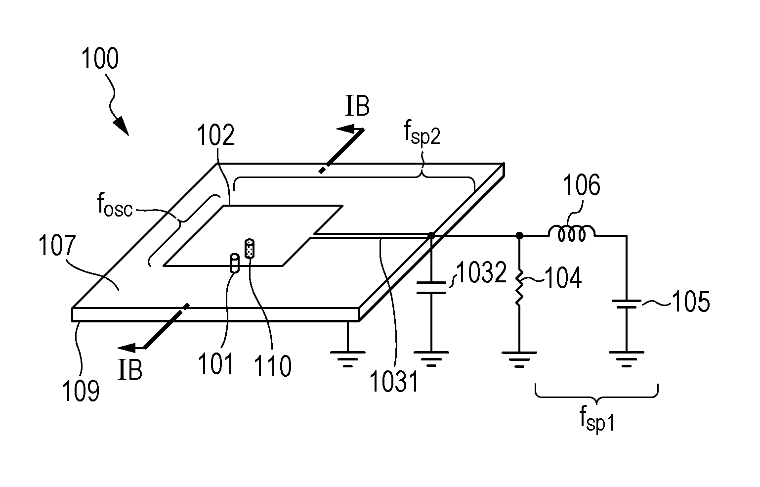
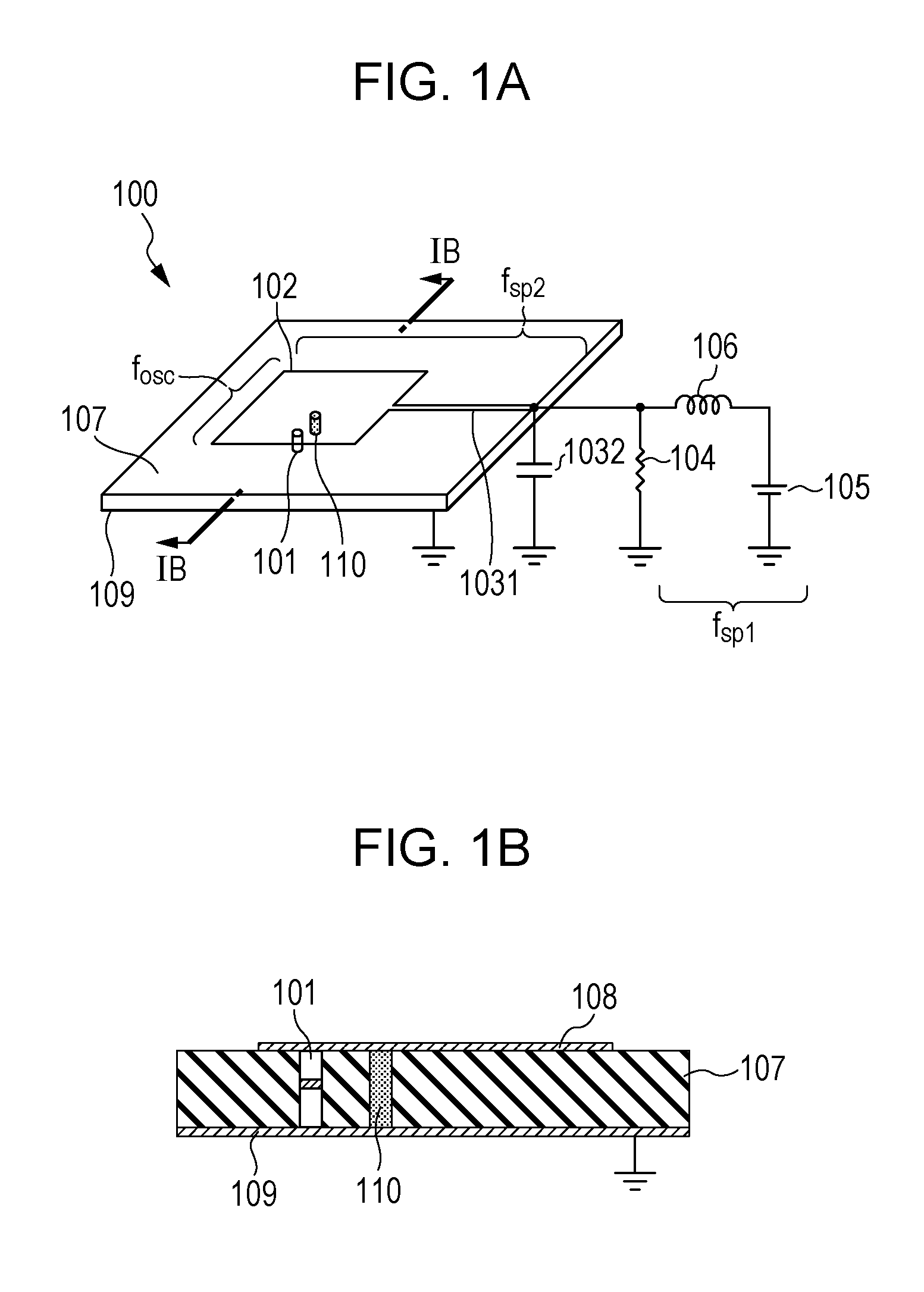
a negative resistance element and oscillator technology, applied in the field of oscillators, can solve the problems of difficult to dispose a low impedance circuit without interfering with the resonator, difficult to employ the techniques of microstrip type resonators, etc., and achieve the effect of stably performing oscillation operations
- Summary
- Abstract
- Description
- Claims
- Application Information
AI Technical Summary
Benefits of technology
Problems solved by technology
Method used
Image
Examples
first example
[0036]The oscillator 200 according to a first example will be described with reference to FIGS. 4A to 4C. The oscillator 200 generates an oscillation frequency fosc of 0.95 THz. In this example, an RTD is used as a negative resistance element 201. The RTD used in this example has a multiple quantum well structure of InGaAs / InAlAs and InGaAs / AlAs and an electrical contact layer of n-InGaAs which are formed on an InP substrate 230. As the multiple quantum well structure, a triple barrier structure is used, for example. More specifically, the multiple quantum well structure is constituted by a semiconductor multilayer structure of AlAs (1.3 nm) / InGaAs (7.6 nm) / InAlAs (2.6 nm) / InGaAs (5.6 nm) / AlAs (1.3 nm). Among them, InGaAs is a well layer, and a lattice-matched InAlAs and lattice-mismatched AlAs are barrier layers. These layers are undoped layers, that is, carrier dope is not intentionally performed on the layers. The multiple quantum well structure is sandwiched between electric con...
second example
[0043]An oscillator 300 according to a second example will be described with reference to FIGS. 6A and 6B. FIG. 6A is a perspective view of the oscillator 300 and FIG. 6B is a sectional view of the oscillator 300 taken along a line VIB. The oscillator 300 generates an oscillation frequency of 0.60 THz. A resonant tunneling diode (RTD) of the first example is used as a negative resistance element 301 and a patch antenna 302 is used as a resonator. Description of configurations the same as those of the first example is omitted.
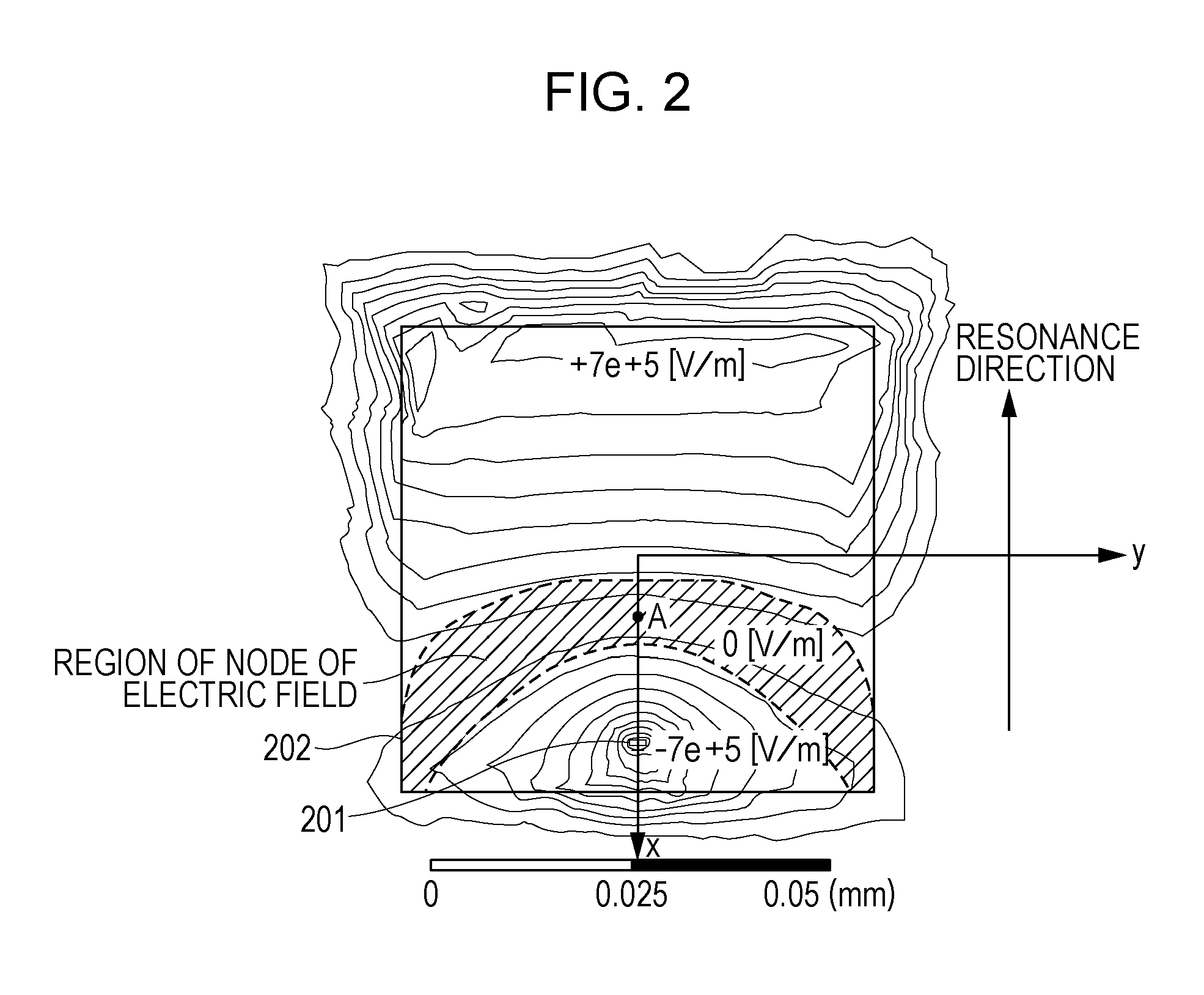
[0044]In the oscillator 300, two resistance elements 310a and 310b are disposed in positions included in a node of a high frequency electric field stably existing in the patch antenna 302. In this way, a plurality of parallel resistors may be disposed in accordance with electric field distribution illustrated in FIG. 2. The patch antenna 302 is a square patch having sides (L) of 150 μm, and a patch conductor 308 is connected to a power source (not illustrated) t...
PUM
 Abstract
Description
Claims
Application Information


