

Insulated metal substrate
a metal substrate and insulating technology, applied in the direction of rigid pipes, cells, surface reaction electrolytic coatings, etc., can solve the problems of negative effects on performance, reliability and the lifetime of the devi
- Summary
- Abstract
- Description
- Claims
- Application Information
AI Technical Summary
Benefits of technology
Problems solved by technology
Method used
Image

Examples
example 1
[0105]Example 1 illustrates the formation of a nanoceramic coating on a metallic substrate that would be suitable for use as the dielectric of an IMS embodying the invention.
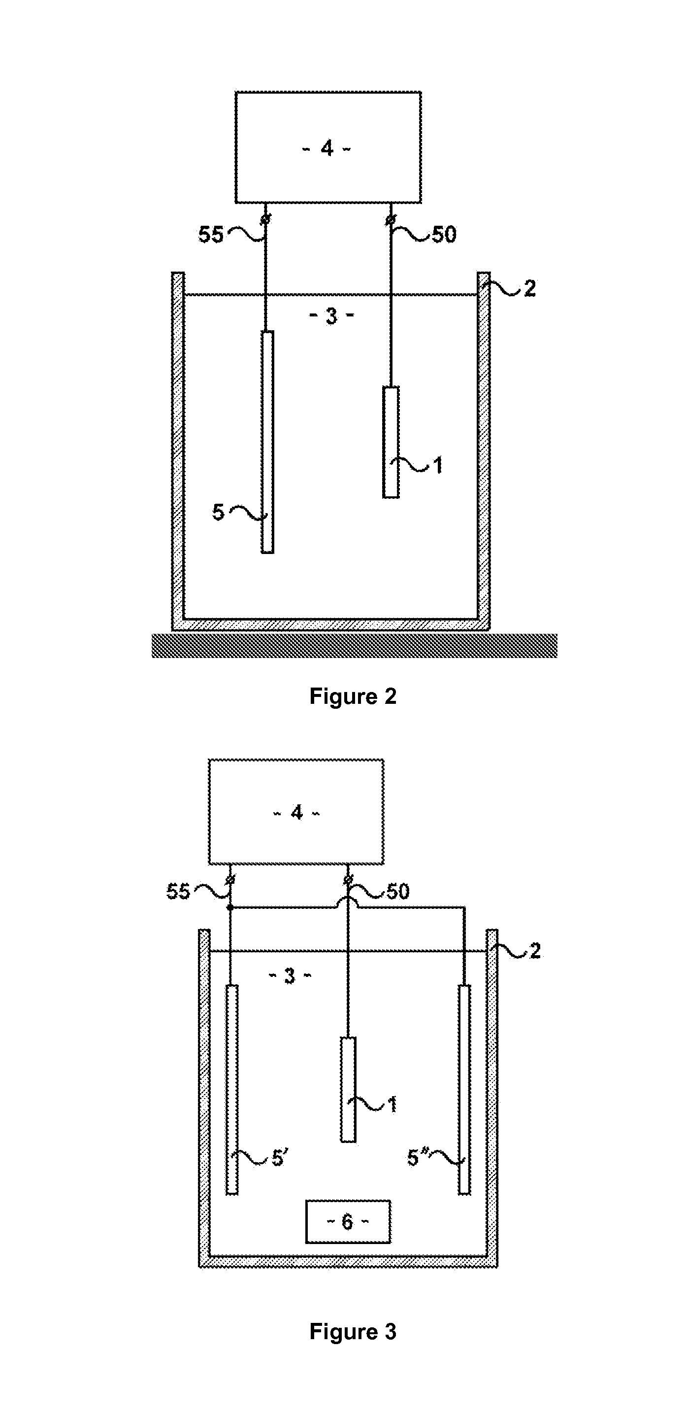
[0106]A substrate in the form of a plate of Al 6082 alloy having dimensions of 50 mm×50 mm×1 mm was treated in an apparatus as described above and illustrated in FIG. 2. The apparatus comprised a tank containing an electrolyte, and the substrate and an electrode were coupled to a pulse power supply as described above and illustrated in FIG. 4. The substrate and the electrode were arranged in contact with the electrolyte.
[0107]The electrolyte was an aqueous solution containing 1.8 g / l of KOH and 1.0 g / l of Alumina particles, forming a stabilised colloidal solution.
[0108]The Pulse Generator applied a sequence of trapezoidally-shaped voltage pulses of alternating polarity between the substrate and the electrode. Positive voltage pulses were applied having a fixed positive voltage amplitude (Va) of 700 V, and negati...
example 2
[0116]FIG. 13 illustrates the use of an IMS embodying the invention as a metal heat sink for a high power device 64 such as for example a high-brightness light-emitting-diode (HB LED) chip. This may be described as a chip on heat sink application.
[0117]A nanoceramic dielectric coating 62 is applied on a flat surface of a metal heat sink 61 to form an IMS. The nanoceramic coating is formed using the method described above in example 1. Metal contact tracks with pads 63 are then formed on the surface of the nanoceramic coating 62.
[0118]The device 64 is attached directly to the nanoceramic coating 62, which provides electrical insulation between the chip and the metal heat sink 61. Contact connectors 65 are attached to connect the device 64 with the contact pads 63. The thickness of the nanoceramic coating is determined by the breakdown voltage requirement of the device, and is grown to the minimum thickness that meets the breakdown voltage requirement. This provides the shortest therm...
example 3
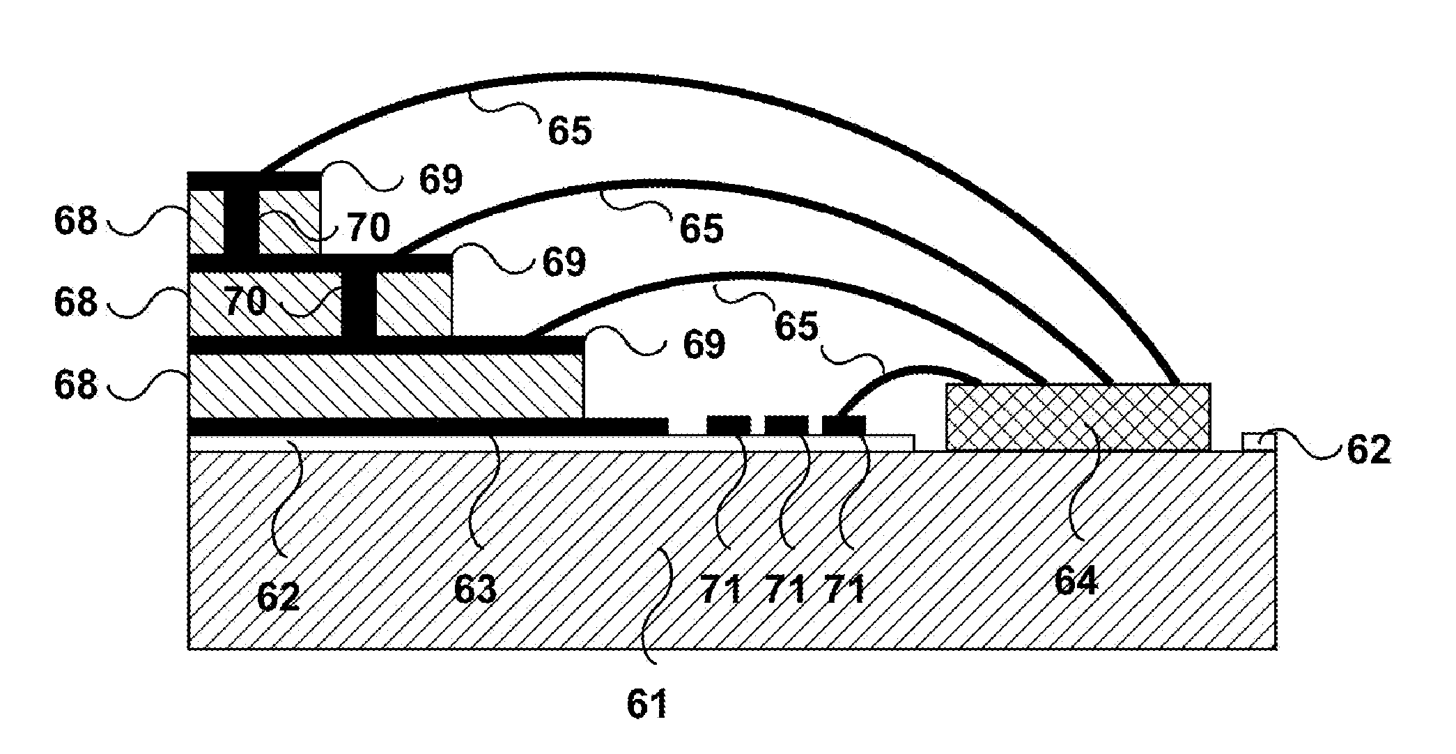
[0119]FIG. 14 illustrates the use of an IMS embodying the invention as a metal heat sink for a packaged device 64, or a chip requiring a low resistance ground path.
[0120]A nanoceramic dielectric coating 62 is applied on a flat surface of a metal heat sink 61 using the method described above in example 1, the metal heat sink 61 acting as a metal substrate for the nanoceramic coating 62. Metal contact tracks with pads 63 and a metal pad 66 are then formed on the surface of the nanoceramic coating 62. Thermal vias 67 defined through the nanoceramic coating 62 have metallic cores that connect the metal pad 66 and the metal heat sink 61.
[0121]The device 64 is attached to the metal pad 66 and contact connectors 65 are attached to contact pads 63.
PUM
| Property | Measurement | Unit |
|---|---|---|
| Grain size | aaaaa | aaaaa |
| Grain size | aaaaa | aaaaa |
| Temperature | aaaaa | aaaaa |
Abstract
Description
Claims
Application Information