Laser processing method

a laser processing and laser technology, applied in semiconductor lasers, semiconductor/solid-state device details, active medium materials, etc., can solve the problems of reducing productivity, affecting reducing the quality of each chip, so as to achieve the effect of greatly improving the productivity

Active Publication Date: 2014-11-13
DISCO CORP
View PDF1 Cites 38 Cited by
  • Summary
  • Abstract
  • Description
  • Claims
  • Application Information

AI Technical Summary

Benefits of technology

[0018]In the laser processing method according to the present invention, the numerical aperture (NA) of the focusing lens for focusing the pulsed laser beam is set so that the value obtained by dividing the numerical aperture (NA) of the focusing lens by the refractive index (N) of the single crystal substrate falls within the range of 0.05 to 0.2. Thereafter, the pulsed laser beam is applied to the single crystal substrate so as to be focused at the focal point set in the single crystal substrate, thereby forming a shield tunnel extending between the focal point and a beam incident surface to which the pulsed laser beam is applied, the shield tunnel being composed of a fine hol

Problems solved by technology

Accordingly, to divide a wafer having a thickness of 300 μm, for example, into individual devices, a plurality of modified layers stacked must be formed along each division line, causing a reduction in productivity.
Accordin

Method used


Image

  • Laser processing method
  • Laser processing method
  • Laser processing method

Examples


example 1-1

[0042]By using a sapphire (Al2O3) substrate (refractive index: 1.7) having a thickness of 1000 μm, the shield tunnel forming step was performed under the following processing conditions to form a shield tunnel, and it was determined whether or not the shield tunnel is good.

[0043]Processing Conditions

[0044]Wavelength: 1030 nm

[0045]Repetition frequency: 50 kHz

[0046]Pulse width: 10 ps

[0047]Average power: 3 W

[0048]Focused spot diameter: 10 μm

[0049]Work feed speed: 500 mm / s

Numerical aperture (NA)Good / poor condition ofof the focusing lensthe shield tunnelS = NA / N0.05Not formed0.1Slightly good0.0580.15Good0.0880.2Good0.1170.25Good0.1470.3Good0.1760.35Slightly good0.2050.4Poor0.45Poor: voids generated0.5Poor: voids generated0.55Poor: voids generated0.6Poor: voids generated

[0050]It is apparent from the above results that in the case of using a sapphire (Al2O3) substrate (refractive index: 1.7) as the single crystal substrate a substantially good shield tunnel can be formed by setting the num...

example 1-2

[0051]By using a silicon carbide (SiC) substrate (refractive index: 2.63) having a thickness of 1000 μm, the shield tunnel forming step was performed under the following processing conditions to form a shield tunnel, and it was determined whether or not the shield tunnel is good.

[0052]Processing Conditions

[0053]Wavelength: 1030 nm

[0054]Repetition frequency:

[0055]Average power: 3 W

[0056]Focused spot diameter: 10 μm

[0057]Work feed speed: 500 mm / s

Numerical aperture (NA)Good / poor condition ofof the focusing lensthe shield tunnelS = NA / N0.05Not formed0.1Not formed0.15Slightly good0.0570.2Good0.0760.25Good0.0950.3Good0.1140.35Good0.1330.4Good0.1530.45Good0.1710.5Good0.190.55Slightly good0.2090.6Poor: voids generated

[0058]It is apparent from the above results that in the case of using a silicon carbide (SiC) substrate (refractive index: 2.63) as the single crystal substrate a substantially good shield tunnel can be formed by setting the numerical aperture (NA) of the focusing lens 422a for...

example 1-3

[0059]By using a gallium nitride (GaN) substrate (refractive index: 2.3) having a thickness of 1000 μm, the shield tunnel forming step was performed under the following processing conditions to form a shield tunnel, and it was determined whether or not the shield tunnel is good.

[0060]Processing Conditions

[0061]Wavelength: 1030 nm

[0062]Repetition frequency: 50 kHz

[0063]Pulse width: 10 ps

[0064]Average power: 3 W

[0065]Focused spot diameter: 10 μm

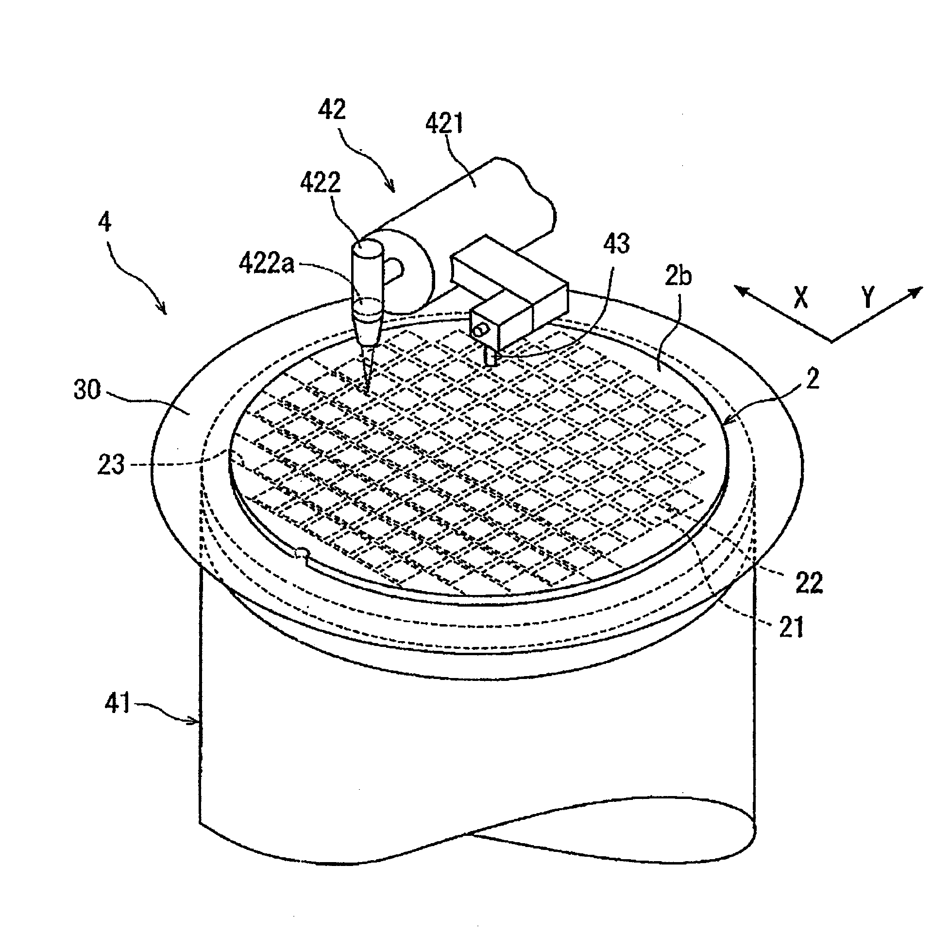
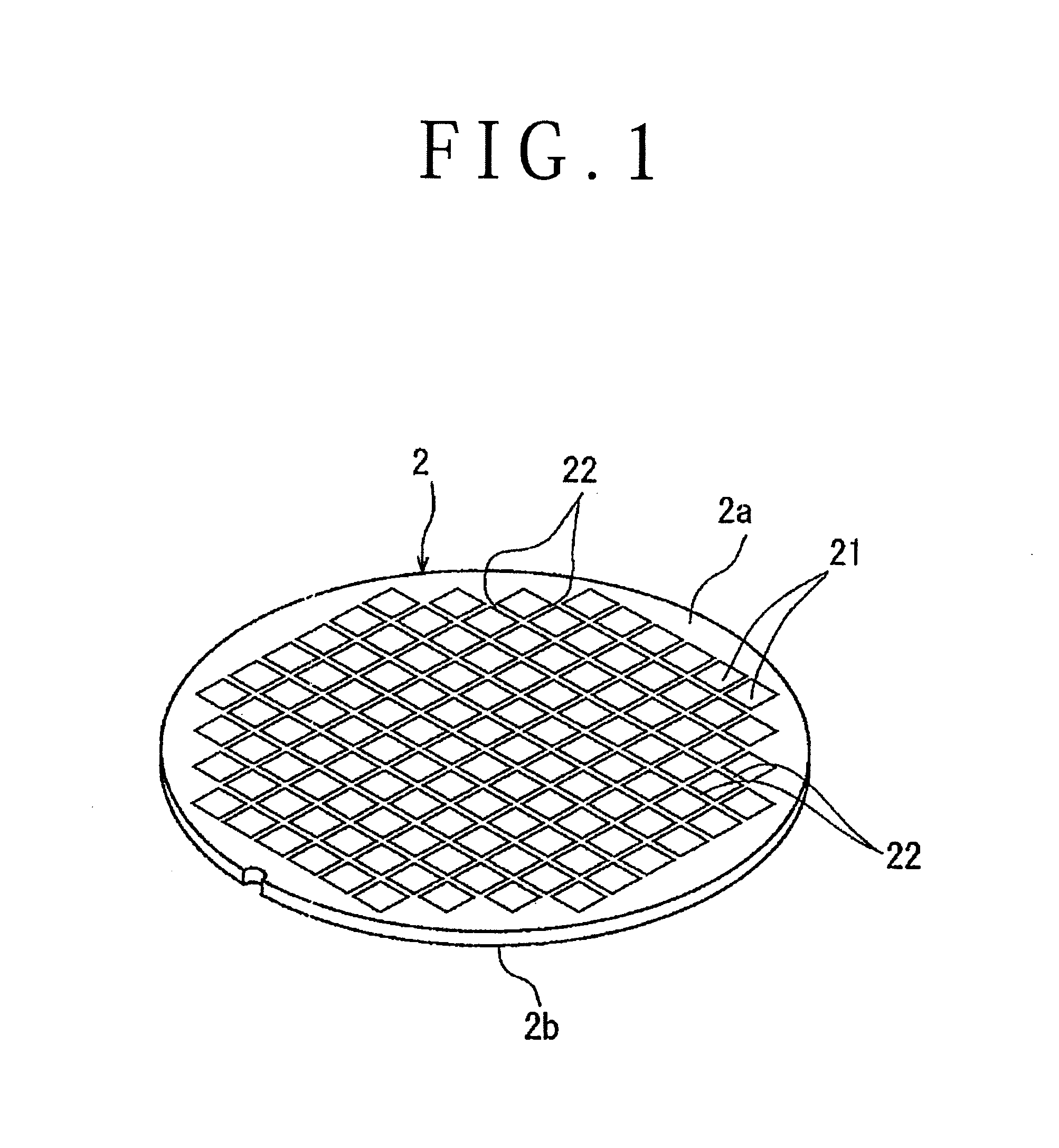
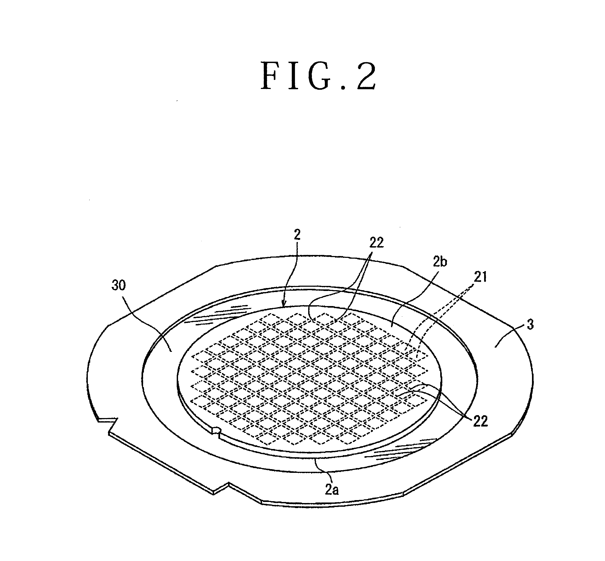
[0066]Work feed speed: 500 mm / s

Numerical aperture (NA)Good / poor condition ofof the focusing lensthe shield tunnelS = NA / N0.05Not formed0.1Slightly good0.0430.15Good0.0650.2Good0.0860.25Good0.1080.3Good0.1300.35Good0.1520.4Good0.1730.45Good0.1950.5Slightly good0.2170.55Poor: voids generated0.6Poor: voids generated

[0067]It is apparent from the above results that in the case of using a gallium nitride (GaN) substrate (refractive index: 2.3) as the single crystal substrate a substantially good shield tunnel can be formed by setting the numerical ap...


PUM

PropertyMeasurementUnit
Energyaaaaaaaaaa
Lengthaaaaaaaaaa
Thicknessaaaaaaaaaa

Abstract

A laser processing method of applying a pulsed laser beam to a single crystal substrate to thereby process the single crystal substrate. The laser processing method includes a numerical aperture setting step of setting the numerical aperture (NA) of a focusing lens for focusing the pulsed laser beam so that the value obtained by dividing the numerical aperture (NA) of the focusing lens by the refractive index (N) of the single crystal substrate falls within the range of 0.05 to 0.2, a positioning step of relatively positioning the focusing lens and the single crystal substrate in the direction along the optical axis of the focusing lens so that the focal point of the pulsed laser beam is set at a desired position in the direction along the thickness of the single crystal substrate, and a shield tunnel forming step of applying the pulsed laser beam to the single crystal substrate so as to focus the pulsed laser beam at the focal point set in the single crystal substrate thereby forming a shield tunnel extending between the focal point and a beam incident surface to which the pulsed laser beam is applied.

Description

BACKGROUND OF THE INVENTION[0001]1. Field of the Invention[0002]The present invention relates to a laser processing method of performing laser processing to a single crystal substrate such as a silicon (Si) substrate, sapphire (Al2O3) substrate, silicon carbide (SiC) substrate, and gallium nitride (GaN) substrate.[0003]2. Description of the Related Art[0004]As well known in the art, in a semiconductor device fabrication process, a functional layer is composed of an insulating film and a functional film is formed on the front side of a silicon (Si) substrate, and a plurality of semiconductor devices such as ICs and LSIs are formed like a matrix from this functional layer, thus obtaining a semiconductor wafer having the plural semiconductor devices. The plural semiconductor devices are partitioned by a plurality of crossing division lines formed on the front side of the semiconductor wafer. The semiconductor wafer is divided along these division lines to obtain the individual semicond...

Claims


Application Information

Patent Timeline
IPC IPC(8): H01S3/10
CPCH01S3/10B23K26/046B23K26/38H01S5/0201H01S5/32341H01S5/0213H01S5/021H01L2924/0002H01L21/78H01L2924/00H01L23/00H01L21/00
Inventor TAKEDA, NOBORUMORIKAZU, HIROSHI
Owner DISCO CORP
Why Eureka
Try Eureka