
P-type oxide, composition for producing p-type oxide, method for producing p-type oxide, semiconductor element, display element, image display device, and system

a technology of p-type oxide and composition, applied in the field of p-type oxide, can solve the problems of difficult control of cu and oxygen content, difficulty in achieving excellent p-type electric conductivity, and difficulty in controlling properties, so as to achieve sufficient electric conductivity, control electric conductivity, and excellent properties

Active Publication Date: 2014-12-04
RICOH KK
View PDF2 Cites 27 Cited by
  • Summary
  • Abstract
  • Description
  • Claims
  • Application Information

AI Technical Summary

Benefits of technology

The present invention offers a new type of p-type oxide that has good electric conductivity and can be easily produced at low temperatures. This oxide can control its electrical conductivity by adjusting the ratio of its components.

Problems solved by technology

One of the reasons why it is difficult to exhibits p-type conductivity is that the valency of Cu and oxygen content are difficult to control.
With such film, excellent p-type electric conductivity cannot be attained, and it is difficult to control properties thereof.
Accordingly, when these p-type oxide materials are used as an active layer of a semiconductor element, properties, such as carrier density and carrier mobility, cannot be optimized.
However, in the disclosed technique, a heat treatment of high temperature, 500° C. or higher, is necessary and therefore it is not suitable for practical use.
Further, control thereof is also insufficient.
As described above, these disclosed techniques have a problem that a p-type oxide material cannot be produced by a practical method, and a p-type oxide that has appropriately controlled and sufficient electric conductivity cannot be provided.
However, this literature does not disclose sufficient information, such as properties of a material of the active layer, a formation method thereof, and properties of the transistor.
In accordance these techniques, however, properties of the active layer cannot be sufficiently controlled, and therefore the electron field-effect mobility and on-off ratio of the TFT have not reached the levels suitable for practical use.
As described above, these disclosed techniques have problems that it is difficult to control properties of the p-type oxide material, such as carrier density, and the properties suitable for use in a device cannot be attained.
So far, it has not yet been discovered a p-type oxide that is effective in practical use.

Method used

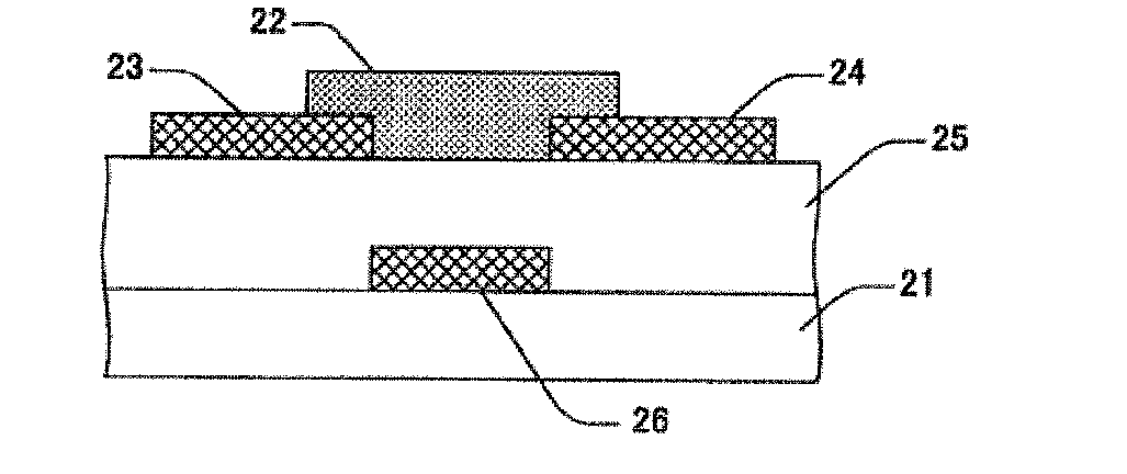
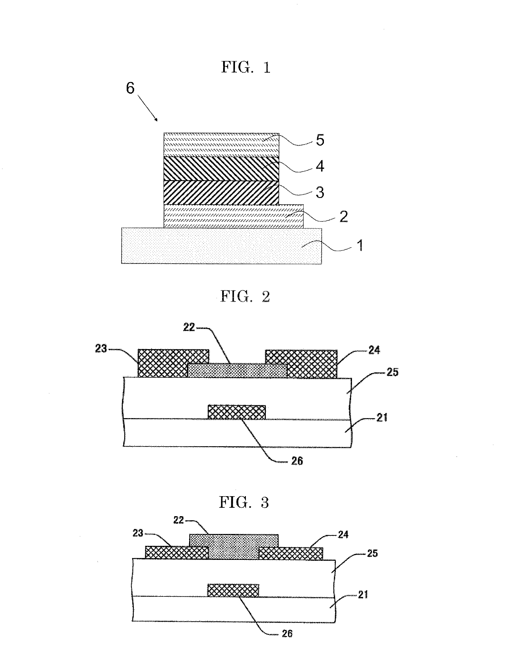
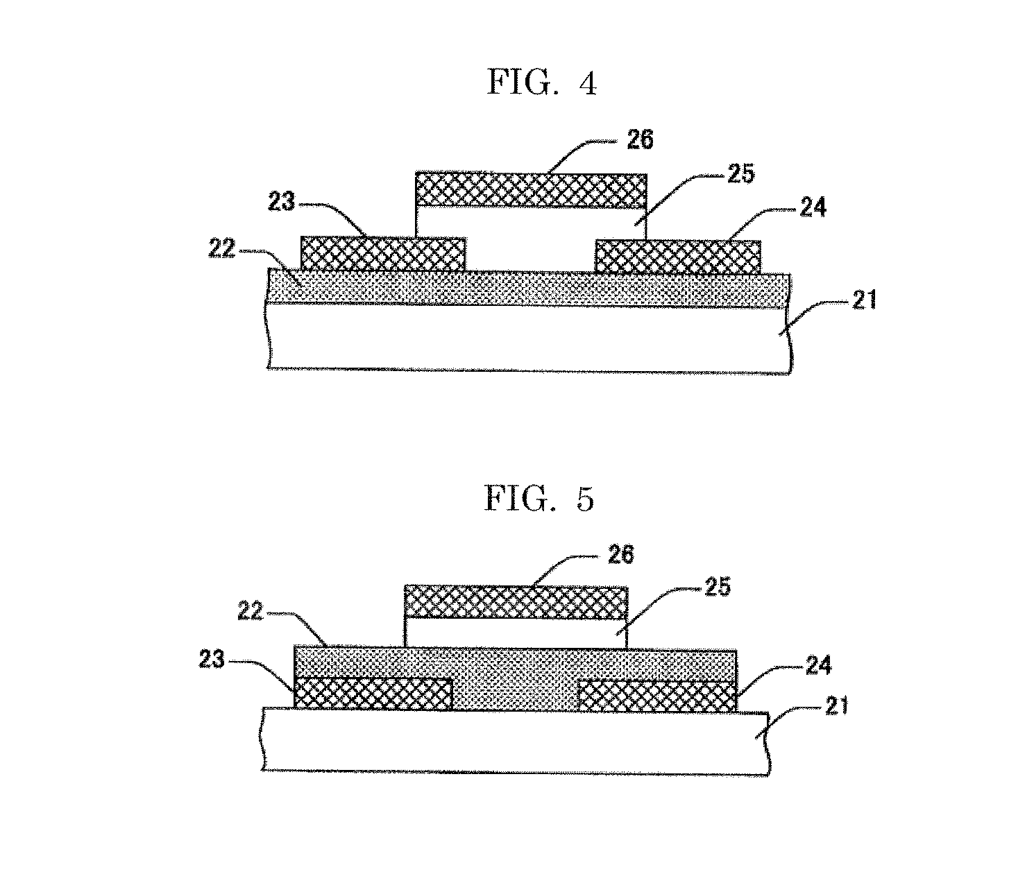

Image

  • P-type oxide, composition for producing p-type oxide, method for producing p-type oxide, semiconductor element, display element, image display device, and system
  • P-type oxide, composition for producing p-type oxide, method for producing p-type oxide, semiconductor element, display element, image display device, and system
  • P-type oxide, composition for producing p-type oxide, method for producing p-type oxide, semiconductor element, display element, image display device, and system

Examples


examples

[0252]Examples of the present invention will be explained hereinafter, but these examples shall not be construed to as limit the scope of the present invention in any way.

examples 1 to 6

Preparation of Cu—Sb Oxide (Amorphous) Film

[0253]Inks for Cu—Sb oxide (compositions for producing a p-type oxide), each of which had the formulation and Sb / Cu molar ratio depicted in Table 1, were prepared. Specifically, a copper neodecanoate (8.28% by mass) toluene solution and a triphenyl antimony (5.83% by mass) toluene solution were blended in accordance with the formulation depicted in Table 1 so that a ratio of Cu moles in a resulting ink to Sb moles in the resulting ink (Sb / Cu molar ratio) was to be 2.5%, 6.3%, 12.5%, 18%, 25%, and 100%, respectively, to thereby prepare 6 different inks for Cu—Sb oxide (compositions for producing a p-type oxide). Note that, 0.5 mL of toluene was added to the formulation depicted in Table 1.

[0254]Next, the ink for Cu—Sb oxide was applied onto a glass substrate by spin coating. After drying the ink for 1 hour at 120° C., the ink was baked for 3 hours at 250° C. while applying light emitted excimer lamp (wavelength: 222 nm) in a flow of oxygen g...

example 7

Production of Cu—Sb Oxide Film (Amorphous)

[0271]In 10 mL of ethylene glycol, 2.42 g (corresponding to 10 mmol) of copper nitrate trihydrate was dissolved to prepare a copper raw material solution. Moreover, 2.29 g (corresponding to 10 mmol) of antimony chloride was dissolved in 10 mL propylene glycol to thereby prepare an antimony raw material solution.

[0272]The copper raw material solution (5 mL) and the antimony raw material solution (0.9 mL) were mixed and stirred to thereby prepare an ink for Cu—Sb oxide (composition for producing a p-type oxide). A ratio of Cu moles in the ink to Sb moles in the ink (Sb / Cu molar ratio) was 18%.

[0273]Next, a glass substrate was coated with the ink for Cu—Sb oxide by spin coating. After drying the ink at 120° C. for 1 hour, the ink was baked at 250° C. for 3 hours while applying light emitted from an excimer lamp (wavelength: 222 nm) in a flow of oxygen gas, to thereby form a Cu—Sb oxide film (p-type oxide film). The Sb / Cu molar ratio in the obta...


PUM


Abstract

To provide is a p-type oxide, including an oxide, wherein the oxide includes: Cu; and an element M, which is selected from p-block elements, and which can be in an equilibrium state, as being present as an ion, wherein the equilibrium state is a state in which there are both a state where all of electrons of p-orbital of an outermost shell are lost, and a state where all of electrons of an outermost shell are lost, and wherein the p-type oxide is amorphous.

Description

TECHNICAL FIELD[0001]The present invention relates to a p-type oxide, a composition for producing the same, a method for producing the same, a semiconductor element, a display element, an image display device, and a system.BACKGROUND ART[0002]Since an announcement of an InGaZnO4 (a-IGZO) thin film transistor (TFT) that exhibits the mobility of a-Si or higher in the amorphous state, researches and developments of oxide semiconductors for practical use have been energetically conducted in all over the world. Most of these oxide semiconductor materials are however n-type oxide semiconductors using electrons as carrier.[0003]If a p-type oxide semiconductor that is comparative to the n-type oxide semiconductor can be utilized on practice, these p-type oxide semiconductor and n-type oxide semiconductor are combined to form p-n junction, to thereby realize a diode, an optical sensor, a solar battery, a LED, or a bipolar transistor. It is also possible to make these devices transparent, as ...

Claims


Application Information

Patent Timeline
IPC IPC(8): H01L29/24H01L27/32H01L21/02H01L27/12G02F1/1368H01L29/786H01L29/861
CPCH01L29/247H01L29/78693H01L27/3244H01L29/861H01L21/02623H01L27/1225G02F1/1368H01L21/02565H01L27/124C01G19/00C01G30/00H01L21/02422H01L21/02483H01L21/02576H01L21/02579H01L21/02628H01L21/02631H01L29/7869C01P2002/72H10K59/12
Inventor ABE, YUKIKOUEDA, NAOYUKINAKAMURA, YUKITAKADA, MIKIKOMATSUMOTO, SHINJISONE, YUJISAOTOME, RYOICHI
Owner RICOH KK
Learn More