Semiconductor Device and Method for Manufacturing the Same

a semiconductor and integrated circuit technology, applied in the direction of semiconductor devices, transistors, electrical equipment, etc., can solve the problems of deterioration or variations of electrical characteristics, decrease in yield of semiconductor integrated circuits, etc., to prevent deterioration of on-state current characteristics, high-integration semiconductor devices, and the effect of reducing the deterioration of yield

Inactive Publication Date: 2014-12-11
SEMICON ENERGY LAB CO LTD
View PDF11 Cites 30 Cited by
  • Summary
  • Abstract
  • Description
  • Claims
  • Application Information

AI Technical Summary

Benefits of technology

[0049]According to one embodiment of the present invention, a semiconductor device can be provided in which deterioration of electrical characteristics that becomes more noticeable as the transistor is miniaturized can be suppressed. Alternatively, a semiconductor device having a structure that can prevent a decrease in yield caused by miniaturization can be provided. Further, a highly integrated semiconductor device can be provided. Another object is to provide a semiconductor device in which deterioration of on-state current characteristics is reduced. Alternatively, a semiconductor device with low power consumption can be provided. Furthermore, a highly reliable semiconductor device can be provided. Alternatively, a semiconductor device in which data is retained even when not powered can be provided.

Problems solved by technology

However, it is known that miniaturization of a transistor causes deterioration or variations of electrical characteristics, such as on-state current, threshold voltage, and a subthreshold value (S value), of the transistor.
This means that miniaturization of a transistor is likely to cause a decrease in yield of a semiconductor integrated circuit.

Method used


Image

  • Semiconductor Device and Method for Manufacturing the Same
  • Semiconductor Device and Method for Manufacturing the Same
  • Semiconductor Device and Method for Manufacturing the Same

Examples


embodiment 1

[0058]In this embodiment, a semiconductor device that is one embodiment of the present invention is described with reference to drawings.

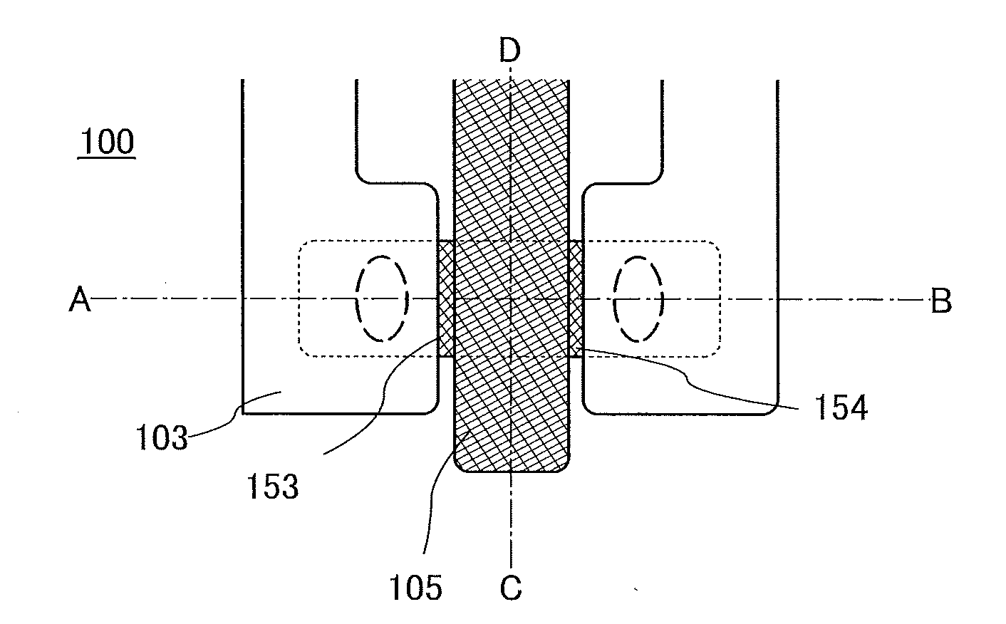
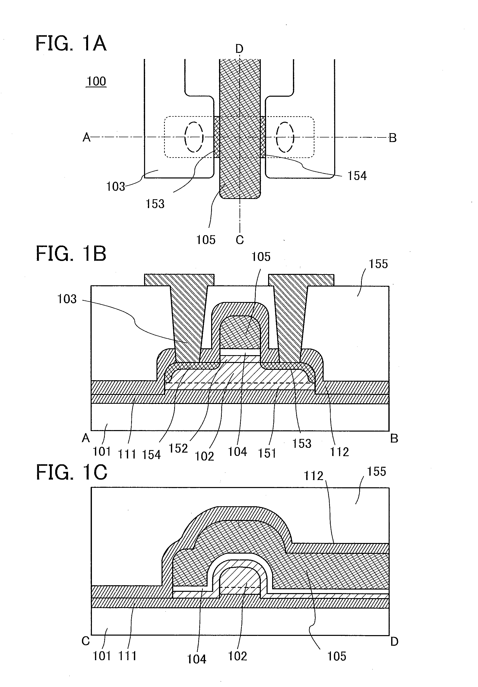
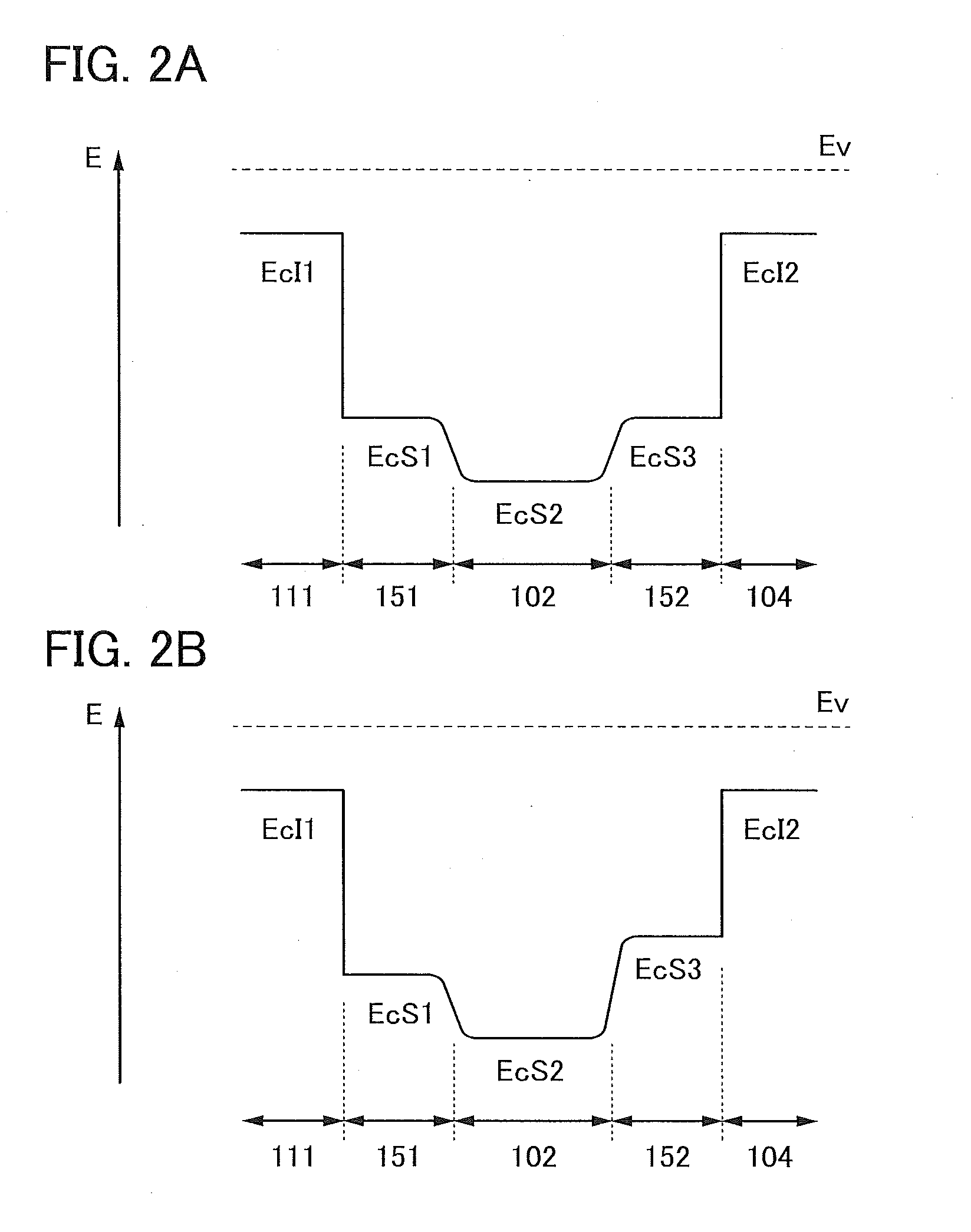
[0059]FIGS. 1A to 1C are a top view and cross-sectional views that illustrate a transistor of one embodiment of the present invention. FIG. 1A is the top view. FIG. 1B illustrates a cross section taken along the dashed-dotted line A-B in FIG. 1A. FIG. 1C illustrates a cross section taken along the dashed-dotted line C-D in FIG. 1A. Note that for simplification of the drawing, some components in the top view in FIG. 1A are not illustrated. In some cases, the direction of the dashed-dotted line A-B is referred to as a channel length direction, and the direction of the dashed-dotted line C-D is referred to as a channel width direction.

[0060]A transistor 100 is formed over a semiconductor substrate 101, and includes a first oxide layer 151; an oxide semiconductor layer 102 including a channel formation region over the first oxide layer 151; low-resista...

embodiment 2

[0086]In this embodiment, an example of a method for manufacturing the transistor 100 described in Embodiment 1 is described below.

[0087]First, the first protective insulating layer 111 is formed over the semiconductor substrate 101.

[0088]The first protective insulating layer 111 can be formed by a sputtering method or the like in an atmosphere containing oxygen, for example. Alternatively, the first protective insulating layer 111 may be formed by a CVD method, a molecular beam epitaxy (MBE) method, an atomic layer deposition (ALD) method, a pulsed laser deposition (PLD) method, or the like in an atmosphere containing oxygen.

[0089]In the case where an aluminum oxide film is used as the first protective insulating layer 111, for example, the first protective insulating layer 111 can be formed in an atmosphere containing oxygen with the use of aluminum oxide as a sputtering target. Note that an inert gas such as a rare gas may be contained in a deposition gas. For example, oxygen is ...

embodiment 3

[0115]In this embodiment, an example of a semiconductor device (storage device) that includes the transistor of one embodiment of the present invention, that can retain stored data even when not powered, and that has an unlimited number of write cycles is described with reference to drawings.

[0116]FIG. 4A is a cross-sectional view of the semiconductor device, and FIG. 4B is a circuit diagram of the semiconductor device.

[0117]The semiconductor device illustrated in FIGS. 4A and 4B includes a transistor 3200 including a first semiconductor material in a lower portion, and a transistor 3300 including a second semiconductor material and a capacitor 3400 in an upper portion. Note that the transistor 100 described in Embodiments 1 and 2 can be used as the transistor 3300.

[0118]One electrode of the capacitor 3400 is formed using the same material as a source electrode layer or a drain electrode layer of the transistor 3300, the other electrode of the capacitor 3400 is formed using the same...


PUM


Abstract

Objects are to obtain a minute transistor by reducing the channel length L of a transistor used in a semiconductor integrated circuit such as an LSI, a CPU, or a memory, increase the operation speed of the circuit, and reduce power consumption. Oxide layers having compositions different from the composition of an oxide semiconductor layer including a channel formation region are provided below and over the oxide semiconductor layer, and in the oxide semiconductor layer including the channel formation region, low-resistance regions are provided to interpose the channel formation region therebetween in the lateral direction. The low-resistance regions are formed in a region other than the channel formation region so as to be in contact with a metal film or a metal oxide film by diffusion of a metal element (e.g., aluminum) contained in the metal or metal oxide films into the parts of the oxide semiconductor layer.

Description

BACKGROUND OF THE INVENTION[0001]1. Field of the Invention[0002]The present invention relates to a semiconductor device including an oxide semiconductor and a method for manufacturing the semiconductor device.[0003]One embodiment of the present invention relates to a semiconductor device including a transistor or a semiconductor device including a circuit including the transistor. For example, one embodiment of the present invention relates to a semiconductor device including a transistor in which an oxide semiconductor is used for a channel formation region or a semiconductor device including a circuit that is formed with the use of such a transistor. For example, the present invention relates to an electronic device that includes, as a component, an LSI, a CPU, a power device mounted in a power circuit, a semiconductor integrated circuit including a memory, a thyristor, a converter, an image sensor, or the like, an electro-optical device typified by a liquid crystal display panel,...

Claims


Application Information

Patent Timeline
Patent Type & Authority Applications(United States)
IPC IPC(8): H01L29/786H01L29/66
CPCH01L29/66969H01L29/7869H01L29/78618
Inventor SUZAWA, HIDEOMI
Owner SEMICON ENERGY LAB CO LTD
Why Eureka
Try Eureka