Semiconductor device

a semiconductor layer and diode technology, applied in the field of pin (i. e., pin) diodes, can solve the problems of restricting the reduction of withstand voltage, and achieve the effects of reducing conduction loss, reducing resistance, and reducing resistance of the second semiconductor layer

Inactive Publication Date: 2015-03-05
DENSO CORP
View PDF13 Cites 15 Cited by
  • Summary
  • Abstract
  • Description
  • Claims
  • Application Information

AI Technical Summary

Benefits of technology

[0015]It is an object of the present disclosure to provide a semiconductor device that reduces the conduction loss without reducing the withstand voltage, and restricts the recovery ringing.
[0017]In the above semiconductor device, since the second semiconductor layer has the carrier density smaller than the spatial charge density, even when the spatial charge density of the second semiconductor layer is increased, the resistance is restricted from being decreased. Accordingly, even in the semiconductor device, in which the drift layer is thinned in order to restrict the conduction loss and the spatial charge density is large in order to restrict the depletion layer from reaching the hole injection layer, the resistance of the second semiconductor layer is larger than a conventional semiconductor device. Thus, the conduction loss is reduced with restricting a recovery ringing in case of recovery. Further, the reduction of the withstand voltage is restricted.
[0018]Alternatively, the second semiconductor layer may provide a level in a frozen region and a level in an extrinsic region. In this case, the temperature dependency of the resistance of the second semiconductor layer is reduced.

Problems solved by technology

Further, the reduction of the withstand voltage is restricted.

Method used


Image

  • Semiconductor device
  • Semiconductor device
  • Semiconductor device

Examples


first embodiment

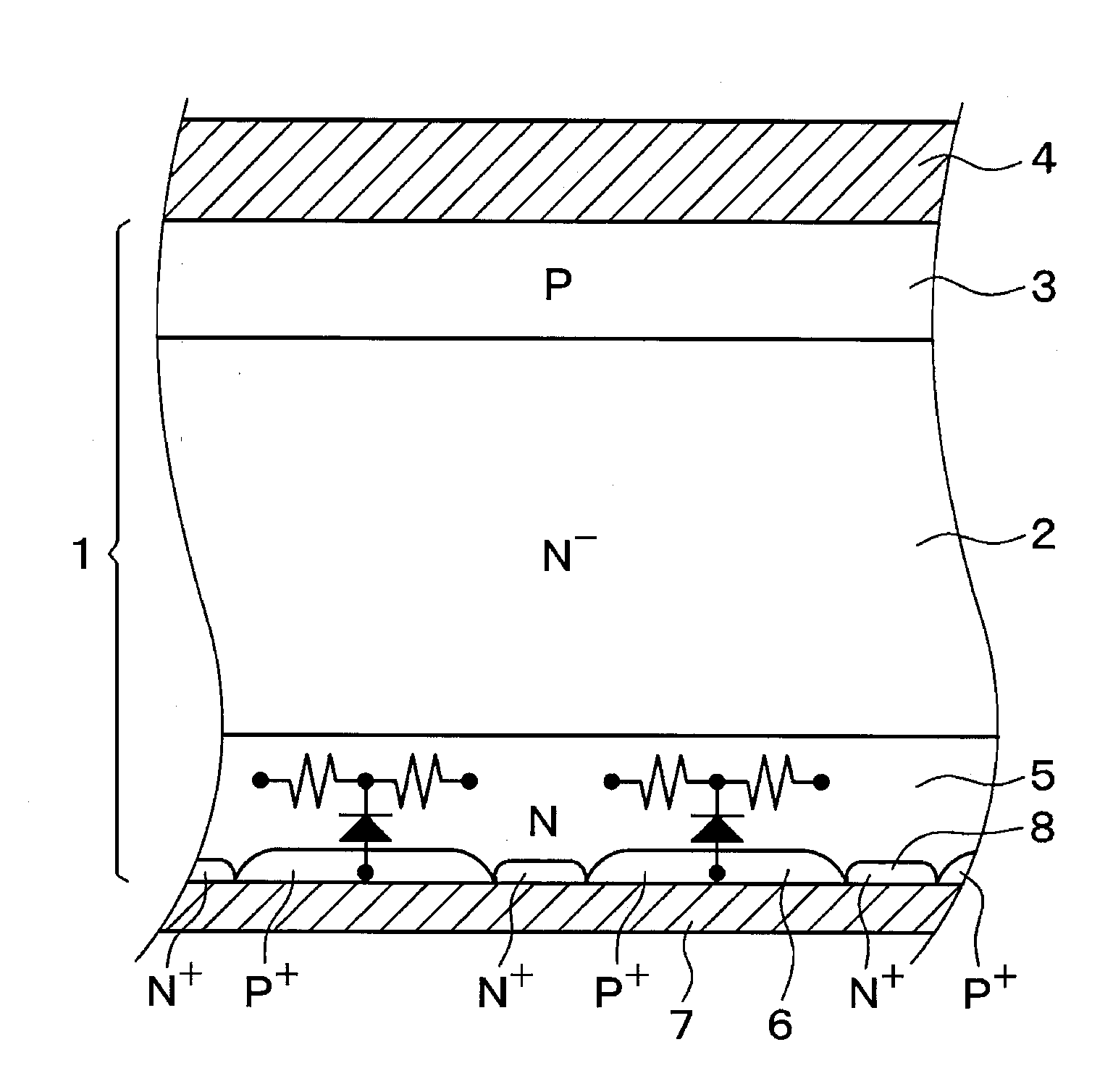
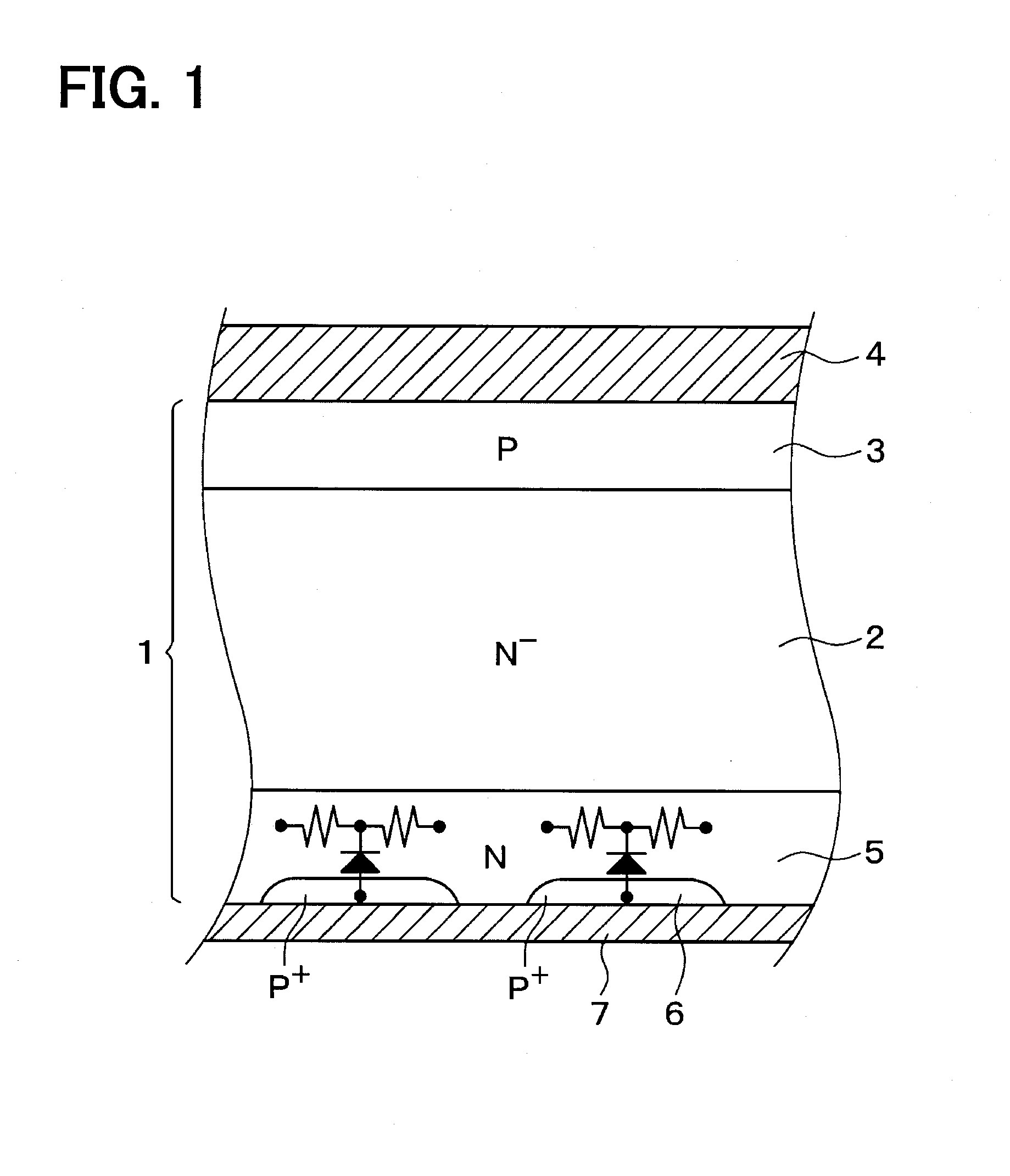
[0022]A first embodiment of the present disclosure will be explained with reference to the drawings. As shown in FIG. 1, the semiconductor device according to the present embodiment is prepared that a pin diode is formed in a semiconductor substrate 1.

[0023]Specifically, the semiconductor substrate 1 includes a drift layer 2 having a N− conductive type. An anode layer 3 having a P conductive type is formed in a surface portion of the drift layer 2, and a carrier density of the anode layer 3 is larger than the drift layer 2. The anode layer 3 is formed such that an impurity such as boron is doped. Specifically, the anode layer 3 has a level providing a 100% activation rate in an operation temperature range of the semiconductor device (e.g., in a range between −40° C. and 15° C.). In other words, the anode layer 3 has the level disposed in an extrinsic region. An anode electrode 4 is formed on the anode layer 3, and the anode electrode 4 is electrically connected to the anode layer 3....

second embodiment

[0036]A second embodiment of the present disclosure will be explained. In the present embodiment, the structure of the cathode layer 5 is changed from the first embodiment. Other features are similar to the first embodiment. Accordingly, the other features are not explained. Here, the cross sectional view of the semiconductor device in the present embodiment is similar to FIG. 1.

[0037]The cathode layer 5 in the present embodiment includes two different levels having different depths. Specifically, the layer 5 includes a level in the frozen region and a level in an extrinsic region in the operation temperature range of the semiconductor device. Here, the level in the extrinsic region is provided by doping phosphorus, arsenicum, antimony or the like.

[0038]In the above case, the temperature dependency of the resistance of the cathode layer 5 is reduced. Specifically, in the level in the frozen region, the carrier density is largely changed with the operation temperature of the semicond...

third embodiment

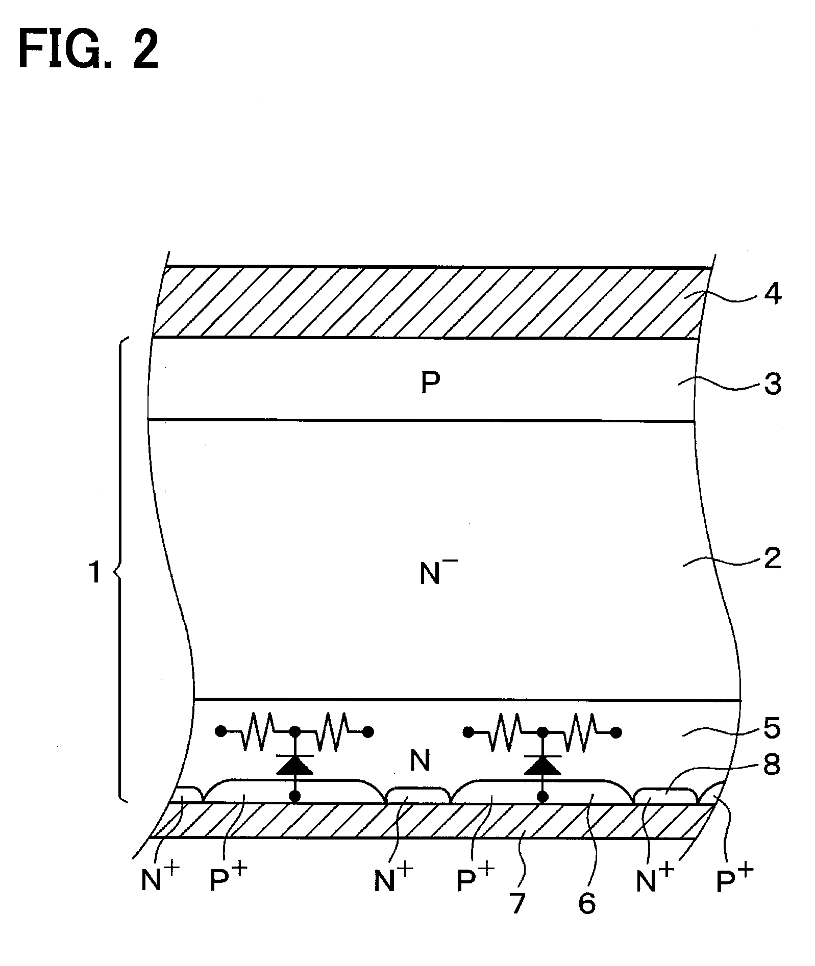
[0041]A third embodiment of the present disclosure will be explained. In the present embodiment, a contact layer is formed in the cathode layer 5 of the first embodiment Other features are similar to the first embodiment. Accordingly, the other features are not explained.

[0042]As shown in FIG. 2, in the present embodiment, a contact layer 8 having a N+ conductive type is formed in a part of the cathode layer, which is sandwiched by the hole injection layer 6, and the contact layer 8 has the carrier density larger than the cathode layer 5. In other words, the hole injection layer 6 and the contact layer 8 are alternately arranged on a side of the cathode layer opposite to the drift layer 2. The cathode layer 7 contacts the hole injection layer 6 and the contact layer 8. The contact layer 8 is prepared by doping phosphorus, arsenicum, antimony or the like.

[0043]In the above case, the contact resistance between the cathode layer 5 (he., the contact layer 8) and the cathode electrode 7 ...


PUM


Abstract

A semiconductor device includes: a drift layer having a first conductive type; a first semiconductor layer having a second conductive type and arranged in a surface portion of the drift layer; a second semiconductor layer having the first conductive type, arranged at a position of the drift layer spaced apart from the first semiconductor layer, and having a carrier density larger than the drift layer; a hole injection layer having the second conductive type and arranged selectively in the second semiconductor layer; a first electrode electrically connecting to the first semiconductor layer; a second electrode electrically connecting to the second semiconductor layer and the hole injection layer. The second semiconductor layer has a carrier density smaller than a spatial charge density.

Description

CROSS REFERENCE TO RELATED APPLICATION[0001]This application is based on Japanese Patent Application No. 2012-106012 filed on May 7, 2012, the disclosure of which is incorporated herein by reference.TECHNICAL FIELD[0002]The present disclosure relates to a pin (i.e., PIN) diode in a semiconductor device.BACKGROUND ART[0003]A semiconductor device having a pin diode, in which a hole injection layer having a P+ conductive type is selectively formed in a cathode layer having a N conductive type, is proposed (for example, please refer to non-patent literature No. 1).[0004]Specifically, in the semiconductor device, the hole injection layer having the P+ conductive type is formed on a side of the cathode layer opposite to a drift layer. A cathode electrode is formed on the cathode layer so as to short-circuit the cathode layer and the hole injection layer. Further, an anode electrode is formed on an anode layer.[0005]In the above semiconductor device, when an electric potential (Le., a forw...

Claims


Application Information

Patent Timeline
Patent Type & Authority Applications(United States)
IPC IPC(8): H01L29/868H01L29/10
CPCH01L29/1095H01L29/868H01L29/08H01L29/861H01L29/8611
Inventor OYAMA, KAZUHIRO
Owner DENSO CORP
Why Eureka
Try Eureka