
Bottom source nmos triggered zener clamp for configuring an ultra-low voltage transient voltage suppressor (TVS)

a transient voltage suppressor and bottom source technology, applied in the direction of diodes, electrical equipment, semiconductor devices, etc., can solve the problems of large area to reduce resistance, uncontrollable high voltage may accidentally strike the circuit, and the diodes are very resistive, so as to improve the structure of the tv device, reduce the voltage, and improve the effect of clamping

Active Publication Date: 2015-03-26
ALPHA & OMEGA SEMICON INC
View PDF27 Cites 17 Cited by
  • Summary
  • Abstract
  • Description
  • Claims
  • Application Information

AI Technical Summary

Benefits of technology

The invention provides a TVS protection circuit with a tunable low trigger voltage of 2.5 volts or lower, and with low leakage and reliable triggering action. This is achieved by implementing a bottom source NMOS triggering Zener clamp, which allows for reliable protection with reduced device area and a simplified configuration. Additionally, the invention provides a TVS protection circuit with a tunable low trigger voltage below 5 volts, which can be manufactured by a simple and cost-effective DMOS type process.

Problems solved by technology

However, in situations such as electrostatic discharge (ESD), electrical fast transients and secondary lightning, an unexpected and an uncontrollable high voltage may accidentally strike onto the circuit.
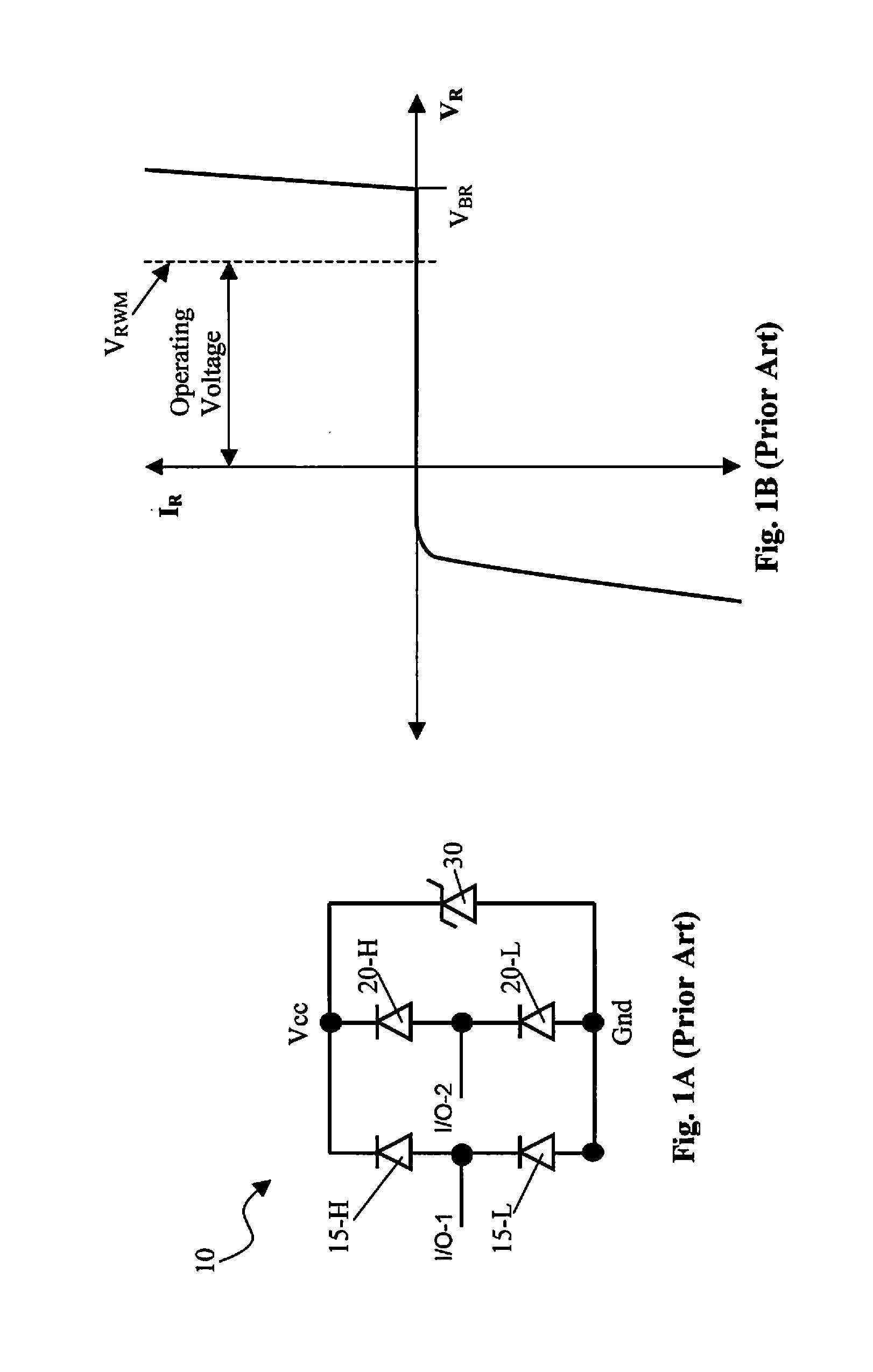
Since the Zener diode has higher resistance per unit area compared with bipolar junction transistors (BJT) or silicon controlled rectifiers (SCR), this is actually a disadvantage at higher currents because the steering diodes also have to be rugged in reverse conduction.
The problem with the Vcc-Gnd clamp diodes is that typically these diodes are very resistive in reverse conduction mode and require large area to reduce resistance.
This is not desirable as high BV not only causes the break down of steering diodes as described above but also causes damage to the circuit the TVS device intends to protect.
The requirement to have large diode size thus limits further miniaturization of a device when such TVS circuit is implemented.
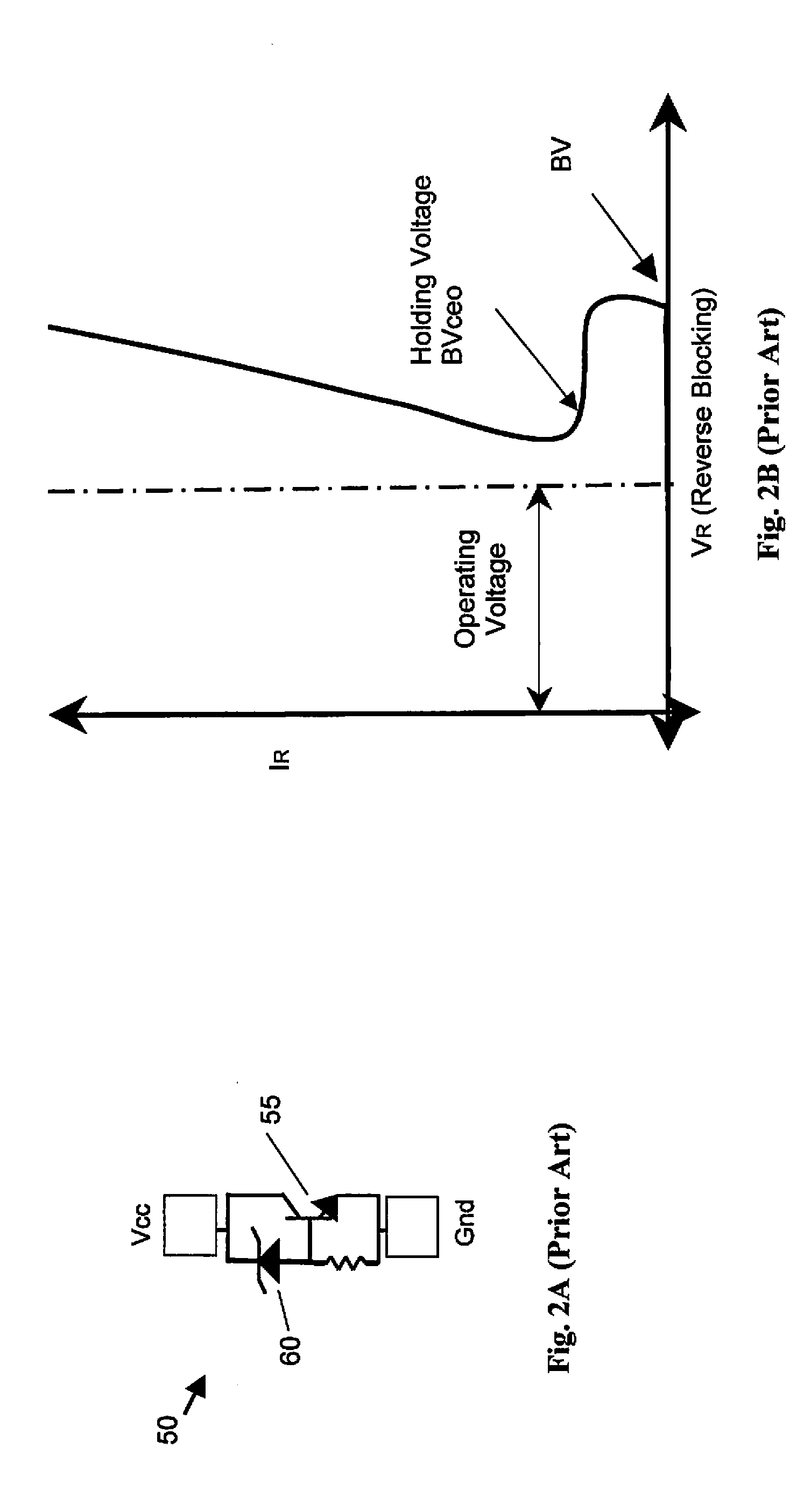
However, in a device that implements a TVS circuit, the snapback phenomenon is not desirable.
The snap-back creates a sudden drop of the reverse voltage that often causes the circuit oscillations due to negative resistance, and can even drop into the operating voltage range, which is undesirable.
However, in addition to the technical difficulties related to the sudden large voltage drops as discussed above, there is a need to reduce the transient voltage protection at a further reduced voltage such as 3.3 volts.
The TVS circuits disclosed have been effective to protective circuit operated at about five volts, however, would not provide the required protection when the operational voltage is further reduced below five volts because of its high triggering and clamping voltage.
However, the MOS-SCR triggered devices have more complicated structure that requires the device to have greater die area.
These types of devices also require IC based manufacturing processes that requires many more masking steps (about 2×-3×) as compared to a DMOS type of process thus resulting in higher production costs.
Additionally, there are concerns with the reliability of JFET based potential barrier triggering mechanism.
In addition, the trigger circuit has many stages, which may affect the overall response time of the TVS circuit: This brings out the need for implementing a simpler device structure that achieves low voltage trigger and clamping and requires a simple fabrication process.

Method used


Image

  • Bottom source nmos triggered zener clamp for configuring an ultra-low voltage transient voltage suppressor (TVS)
  • Bottom source nmos triggered zener clamp for configuring an ultra-low voltage transient voltage suppressor (TVS)
  • Bottom source nmos triggered zener clamp for configuring an ultra-low voltage transient voltage suppressor (TVS)

Examples


Embodiment Construction

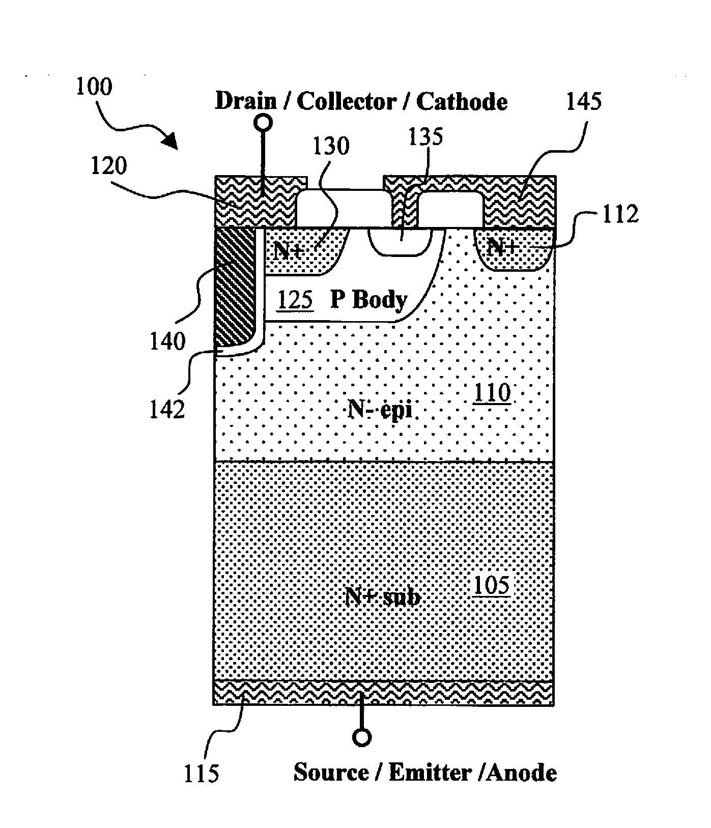
[0033]FIGS. 4A and 4B show a cross sectional view and the corresponding equivalent circuit elements respectively of a TVS device 100 of this invention. FIG. 4C is an I-V diagram that shows the current conduction and voltage characteristics of the TVS device 100. The TVS device 100 is formed in a N+ substrate 105 supporting a N-epitaxial layer 110 thereon with a anode terminal 115 disposed on the bottom and an cathode terminal 120 disposed on the top surface of the substrate that is contacted to a N+ drain / collector region 130. In addition to a TVS diode 150, the device also contains a NMOSFET 160 and a NPN bipolar transistor 170, as shown in the equivalent circuit 100. The connectivity of the terminals of the NMOS 160 and NPN bipolar transistor 170 in this structure are explained next. The TVS device-structure 100 includes a surface P+ body contact region 135 on top of a P-body region 125. The surface P+ body contact region 135 is connected to the anode / source / emitter terminal using...


PUM

PropertyMeasurementUnit
voltageaaaaaaaaaa
voltageaaaaaaaaaa
voltageaaaaaaaaaa

Abstract

A low voltage transient voltage suppressing (TVS) device supported on a semiconductor substrate supporting an epitaxial layer to form a bottom-source metal oxide semiconductor field effect transistor (BS-MOSFET) that comprises a trench gate surrounded by a drain region encompassed in a body region disposed near a top surface of the semiconductor substrate. The drain region interfaces with the body region constituting a junction diode. The drain region on top of the epitaxial layer constituting a bipolar transistor with a top electrode disposed on the top surface of the semiconductor functioning as a drain / collector terminal and a bottom electrode disposed on a bottom surface of the semiconductor substrate functioning as a source / emitter electrode. The body regions further comprises a surface body contact region electrically connected to a body-to-source short-connection thus connecting the body region to the bottom electrode functioning as the source / emitter terminal.

Description

[0001]This Patent Application is a Divisional Application and claims the Priority Date of a co-pending application Ser. No. 12 / 456,555 filed by common inventors of this Application on Jun. 17, 2009. The Disclosures made in these applications Ser. No. 12 / 456,555 are hereby incorporated by reference.BACKGROUND OF THE INVENTION[0002]1. Field of the Invention[0003]The invention relates generally to a circuit configuration and method of manufacturing a transient voltage suppressor (TVS). More particularly, this invention relates to an improved circuit configuration and method of manufacturing an improved transient voltage suppressor (TVS) for low voltage protection by implementing a bottom source NMOS triggered Zener clamp configuration in the TVS circuit.[0004]2. Description of the Relevant Art[0005]The transient voltage suppressors (TVS) are commonly applied for protecting integrated circuits from damages due to the inadvertent occurrence of an over voltage imposed onto the integrated ...

Claims


Application Information

Patent Timeline
Patent Type & Authority Applications(United States)
IPC IPC(8): H01L29/78H01L29/70H01L29/66
CPCH01L29/7827H01L29/66234H01L29/70H01L29/66666H01L29/7813H01L29/66734H01L29/7804H01L29/7808H01L29/781H01L29/732H01L29/7327H01L21/8249H01L29/6628H01L27/0716
Inventor BOBDE, MADHUR
Owner ALPHA & OMEGA SEMICON INC
Learn More