

Method for manufacturing modular microfluidic paper chips using inkjet printing
a microfluidic paper and inkjet printing technology, applied in the direction of positive displacement liquid engines, instruments, glassware, etc., can solve the problems of complex patterning process, high cost of apparatus and chemicals used, and high environmental pollution, so as to achieve simple method, reduce environmental pollution, and improve environmental protection
- Summary
- Abstract
- Description
- Claims
- Application Information
AI Technical Summary
Benefits of technology
Problems solved by technology
Method used
Image

Examples
example 1
Preparing Carbon Nanotube (CNT) Ink
[0066]In order to print electrode patterns, an ink was prepared using CNTs, and the ink was printed on paper and then used as an electrode. In order to print the CNT electrodes using an inkjet printer, first, a dispersant was put in multi-wall CNTs, followed by ball milling, thereby preparing a CNT ink dispersed in water. The electrode was printed by an inkjet printer using the ink, and then a surface of the printed electrode was observed by an electron scanning microscope. The results showed that the CNT ink prepared in the present invention uniformly packs the paper (FIG. 2B).
[0067]Meanwhile, the electrode is required to have a predetermined level of conductivity to perform a function thereof. In the present invention, the CNT electrode had 1 kΩ / sq on a general A4 paper and 200 Ω / sq on a photograph printing paper, and thus exhibited conductivity sufficient to be used as an electrode.
example 2
Producing DLTMC Patterns of Digital Microfluidic Paper Chip Using Carbon Nanotube (CNT) Ink
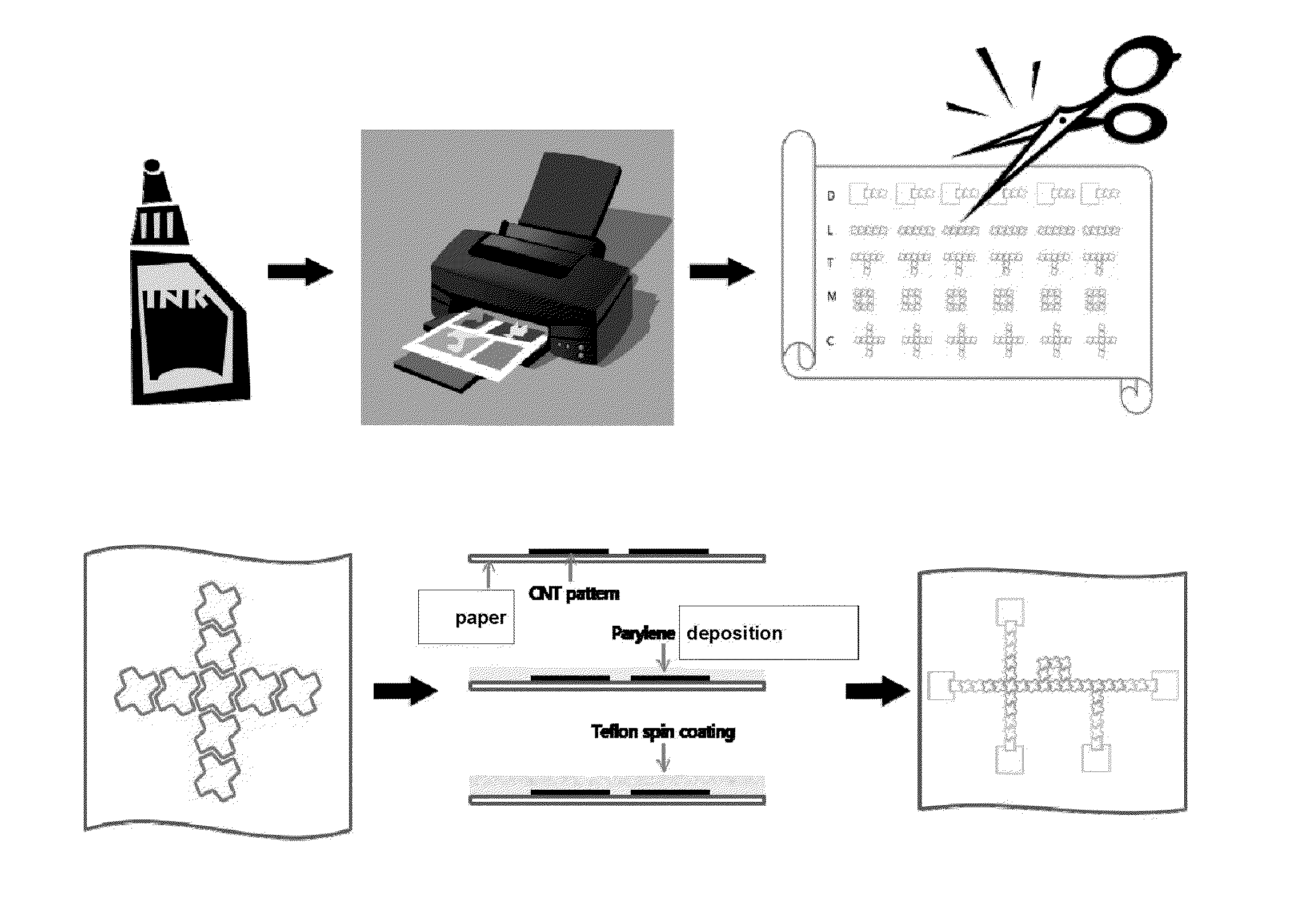
[0068]In order to produce an electrode pattern to be used in manufacturing a digital microfluidic paper chip, the drawing was made using a program, such as Photoshop or CAD, and an electrode with a desired shape was printed on general A4 paper or photograph printing paper at a resolution of several tens of μm by using the CNT ink and an inkjet printer.
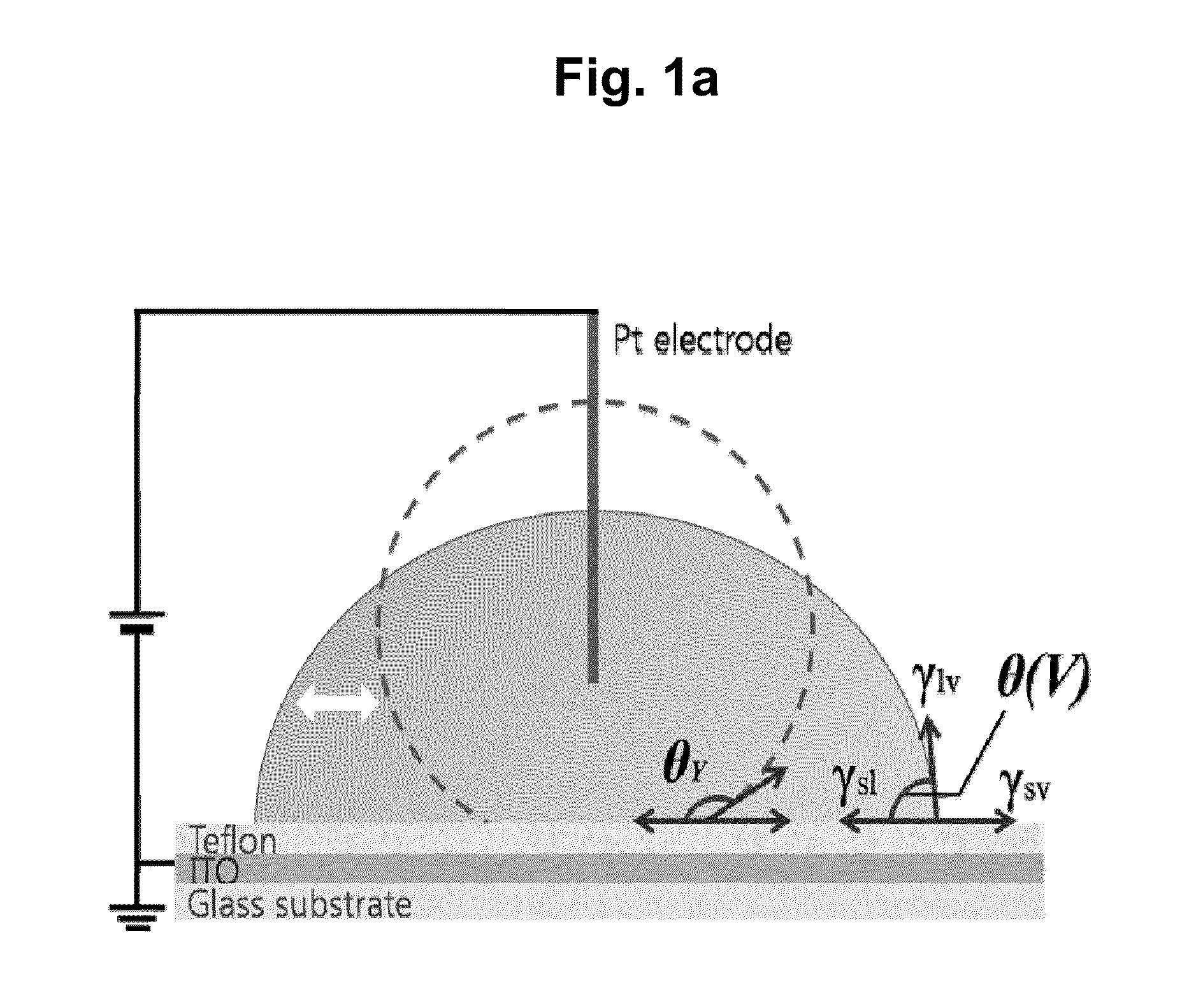
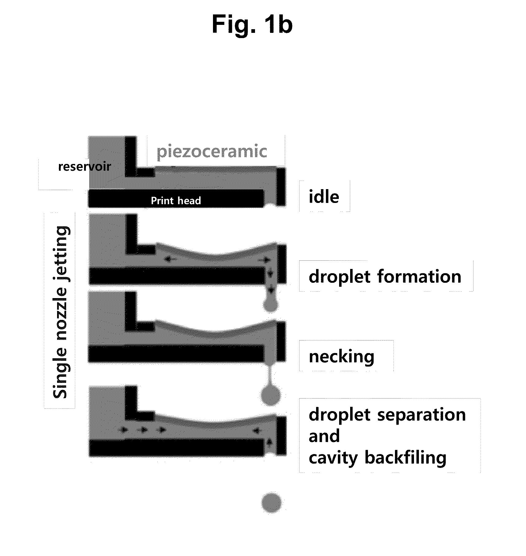
[0069]After that, necessary electrode patterns were cut from the printed paper, followed by patterning, and in order to form an insulating layer thereon, parylene C was deposited and Teflon AF1600 was spin-coated. In the case where a water droplet was dropped on the electrode patterns of the paper chip, on which the parylene C and Teflon were deposited, and then a voltage (V) was applied thereto, it was confirmed that the movement of the water droplet on a surface of the chip can be controlled as shown in FIG. 4A. FIG. 4B shows the driving behavi...
example 3
Module Chip Combined with CMT Patterns and Synthesis of Gold Nanoparticles Using Same
[0071]A module chip combined with CMT patterns was assembled by using five D patterns and one of each for C, M, and T patterns. Gold nanoparticles were synthesized by using the patterns and three kinds of solutions (HAuCl4, NaBH4, and lysine). FIG. 5 shows an assembly example of a module chip combined with CMT patterns, and table 2 shows an operation and a gold nanoparticle synthesis step at each site along the moving route of fluid on a module chip combined with CMT patterns.
TABLE 2Synthesis of gold nanoparticlesStepOperationDescription1A HAuCl4 solution from ① and a NaBH4 solution from ② meet each other, and then merge at a +-shaped site. 2The merged solutions mix with each other while rotating along a □-shaped pattern (colloidal gold nanoparticles are formed). 3A lysine solution as a capping reagent comes out from ③, and then meets the solutions of step 2. 4Droplets made in step 3 mix with each o...
PUM
| Property | Measurement | Unit |
|---|---|---|
| voltages | aaaaa | aaaaa |
| voltages | aaaaa | aaaaa |
| distance | aaaaa | aaaaa |
Abstract
Description
Claims
Application Information