
Reconfigurable circuit, storage device, and electronic device including storage device

a technology of reconfigurable circuits and storage devices, applied in logic circuit coupling/interface arrangements, instruments, pulse techniques, etc., can solve the problems of inconvenient application of flash memory, inability to start normal operation, and large size of table ram, so as to increase the manufacturing cost of storage devices, shorten the test time in product shipment, and facilitate configuration

Active Publication Date: 2015-05-07
SEMICON ENERGY LAB CO LTD
View PDF6 Cites 3 Cited by
  • Summary
  • Abstract
  • Description
  • Claims
  • Application Information

AI Technical Summary

Benefits of technology

The present invention provides a novel semiconductor device, a method for driving and testing it, that can perform easy configuration, have a short startup time, be cost-effective while still being efficient. The semiconductor device can be a reconfigurable circuit or a storage device with a redundant circuit or a test circuit. Additionally, it can be used to replace defective memory cells with a redundant memory cell and effectively utilize memory capacity.

Problems solved by technology

Thus, the table RAM size is huge.
Furthermore, it takes time to start normal operation after startup; thus, the flash memory is not suitable for an application that is frequently powered off to reduce power consumption, such as a mobile device.
However, since the test circuit is not needed after product shipment, a high-performance test circuit leads to an increase in the manufacturing cost of the storage device.

Method used

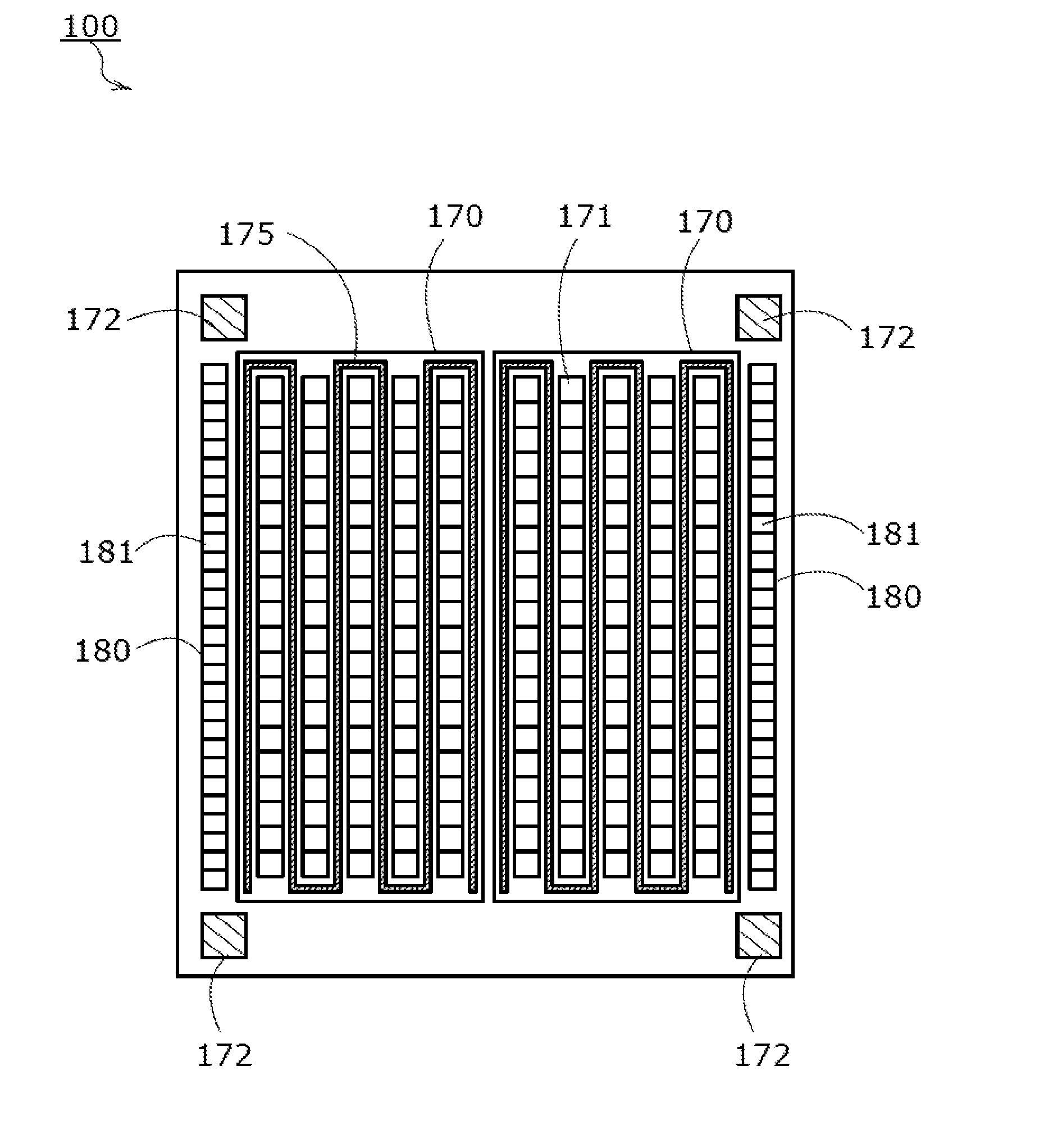

Image

  • Reconfigurable circuit, storage device, and electronic device including storage device
  • Reconfigurable circuit, storage device, and electronic device including storage device
  • Reconfigurable circuit, storage device, and electronic device including storage device

Examples


embodiment 1

[0034]In this embodiment, a reconfigurable circuit is described.

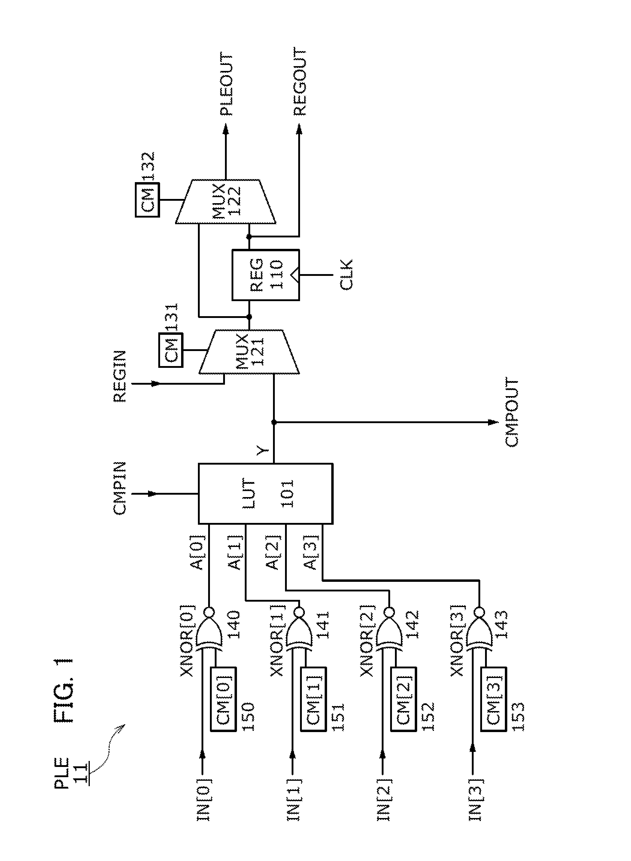
[0035]First, structure examples of PLEs are described. The PLE forms a basic logic block (basic logic cell) of a logic portion in a reconfigurable circuit. The PLE itself is also a reconfigurable circuit, which includes at least a look-up table (LUT) for outputting one data value in response to a plurality of input values, a register for storing data, and a configuration memory for storing configuration data.

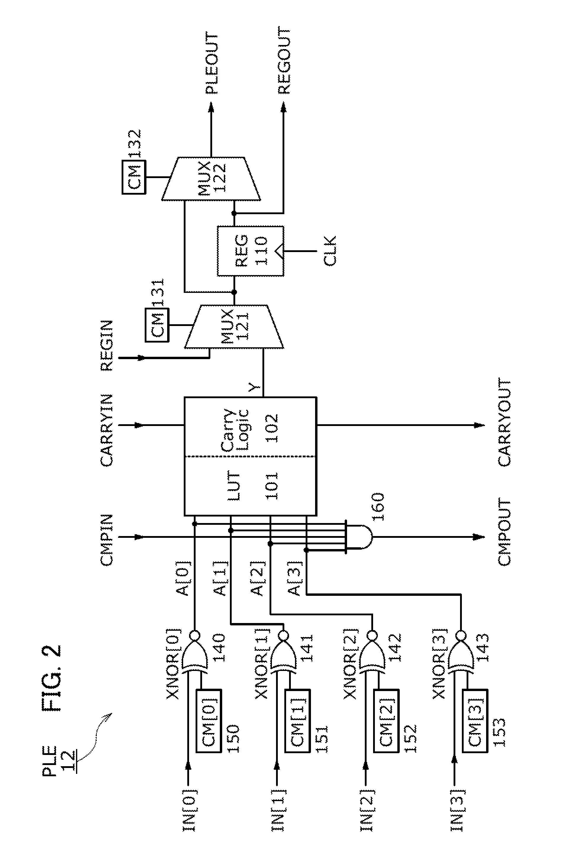
[0036]The reconfigurable circuit includes, for example, a logic array in which a plurality of PLEs are arranged in an array, wirings, and a switch circuit for controlling connection between the wiring and the PLE. A plurality of logic array portions can be provided in the reconfigurable circuit. As described later, in the logic array, registers in adjacent PLEs are cascaded to form a register chain. In the case where carry logic circuits are provided in the PLEs, a carry chain can be formed by cascading the carry lo...

embodiment 2

[0064]In this embodiment, a storage device, especially, a storage device including a redundant circuit is described.

[0065]FIG. 4 is a block diagram illustrating a structure example of a storage device.

[0066]A storage device 20 includes a memory portion 200 and a reconfigurable circuit (RCFGC) 250. The RCFGC 250 functions as a redundant circuit.

[0067]The memory portion 200 includes a memory cell array 210 and a peripheral circuit 220. The memory cell array 210 is a circuit in which a plurality of memory cells are arranged in an array. The position of each memory cell can be specified by its address. The memory cell array 210 has a function of controlling writing and reading data to and from the memory cell array 210 in response to control signals CE, WE, and RE, address data ADDR, and the like from the outside and a function of controlling data transmission and reception to and from the outside.

[0068]There is no particular limitation on the structure of the memory portion 200. For ex...

embodiment 3

[0099]The reconfigurable circuit in Embodiment 1 can be used as processors (e.g., CPUs, microcontrollers, and wireless chips) in a wide variety of fields, such as digital signal processing, software-defined radio systems, avionic systems (electronic devices used in aircraft, such as communication systems, navigation systems, autopilot systems, and flight management systems), ASIC prototyping, medical image processing, voice recognition, encryption, bioinformatics, emulators for mechanical systems, and radio telescopes in radio astronomy.

[0100]The storage device in Embodiment 2 can be used as a storage device such as a USB memory, an SD memory card, or a solid state drive (SSD). Alternatively, the storage device in Embodiment 2 can be used as a storage of a main memory in a processor such as a CPU, a microcontroller, or a wireless chip (e.g., an RFID tag). When an arithmetic processing portion such as a CPU core, a storage device, an input / output circuit, and the like are included in...


PUM


Abstract

A reconfigurable circuit suitable for a redundant circuit of a storage device is provided. A programmable logic element (PLE) includes k logic circuits (e.g., XNOR circuits), k configuration memories (CM), and another logic circuit (e.g., an AND circuit) to which the outputs of the k logic circuits are input. The output of the AND circuit represents whether k input data of the PLE all correspond to configuration data stored in the k CMs. For example, when the address of a defective block in the storage device is stored in the CM and address data of the storage device the access of which is requested is input to the PLE, whether the defective block is accessible can be determined from the output of the AND circuit.

Description

BACKGROUND OF THE INVENTION[0001]1. Field of the Invention[0002]The present invention relates to an object, a method, or a manufacturing method. In addition, the present invention relates to a process, a machine, manufacture, or a composition of matter. For example, the present invention relates to a semiconductor device, a method for driving the semiconductor device, or a method for testing the semiconductor device. Specifically, the present invention relates to a reconfigurable circuit, a method for driving the reconfigurable circuit, a storage device, or a method for testing the storage device.[0003]2. Description of the Related Art[0004]To improve the manufacturing yield of a storage device such as a flash memory, a storage device in which a redundant memory cell is prepared and a redundant circuit for replacing a defective memory cell with the redundant memory cell is provided has been proposed. In addition, a storage device in which a specific test circuit is included to test ...

Claims


Application Information

Patent Timeline
Patent Type & Authority Applications(United States)
IPC IPC(8): H03K19/003H03K19/20H03K19/0175
CPCH03K19/00392H03K19/20H03K19/017581H03K19/0075H03K19/1737H03K19/17728H03K19/1776H03K19/21G11C29/08
Inventor KUROKAWA, YOSHIYUKI
Owner SEMICON ENERGY LAB CO LTD
Learn More